Introduction to Electrical and Electronics Engineering. Module 1, module 1.

GXEST104 · 185 pages · Your place is saved in this browser

Contents · Resistor
  1. Resistor
  2. V-I characteristics
  3. Capacitor
  4. V-I relation of capacitor
  5. Inductance
  6. V-I characteristic
  7. Inductor (L)
  8. constant Voltage source
  9. Behavior on load
  10. Behavior on Short Circuit
  11. Behavior on Open Circuit:
  12. Ideal voltage source
  13. V-I characteristic
  14. Constant Current Source
  15. Behavior on Open Circuit:
  16. V-I characteristic
  17. SI units of electrical quantities
  18. Series and parallel connection
  19. Meaning of NETWORK & CIRCUIT
  20. Ohm's law
  21. German physicist and mathematician Georg Simon Ohm
  22. 1.6 Resistances in series Based on ohms law
  23. 1.7 Resistances in parallel
  24. Application of ohms law
  25. Application 1
  26. Voltage Divider Rule
  27. Current Divider Rule
  28. Important note
  29. Application 2
  30. Source transformation rule
  31. Important points
  32. Circuit vs Network
  33. Relative potential
  34. Finding Loops in a Circuit
  35. Mesh
  36. Kirchhoff'S Voltage Law
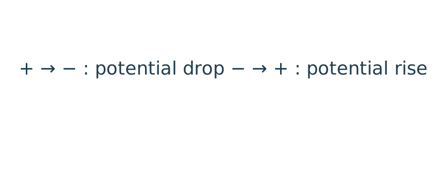
  37. Polarities
  38. Sign convention for applying signs to the voltage polarities in our KVL equations
  39. Example kvl equation
  40. Super mesh(note)
  41. points (Super mesh )
  42. 3. Solving the system of equations
  43. 2.6.1 Matrix method of analysis
  44. Matrix form RULE
  45. Kirchhoff'S Current Law
  46. k.c.l Version 2
  47. Find node voltages
  48. Node voltage method step
  49. Nodal voltage Matrix representation
  50. Compare mesh current matrix node voltage matrix
  51. Mesh Analysis
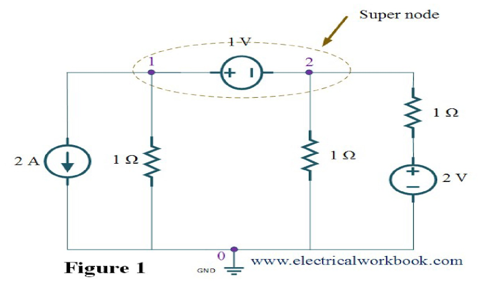
  52. Nodal Analysis
  53. Next problem
  54. Super node-procedure
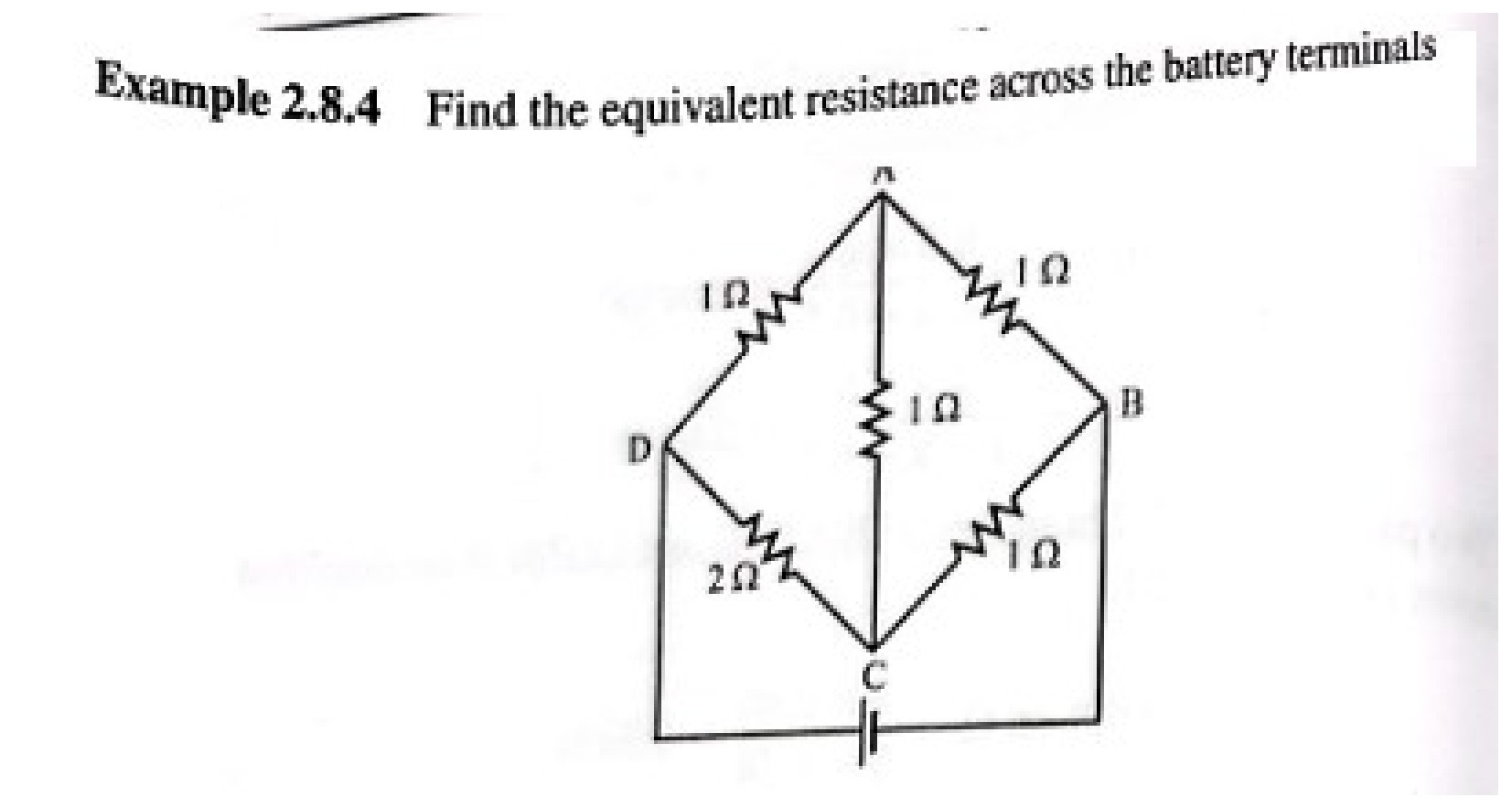
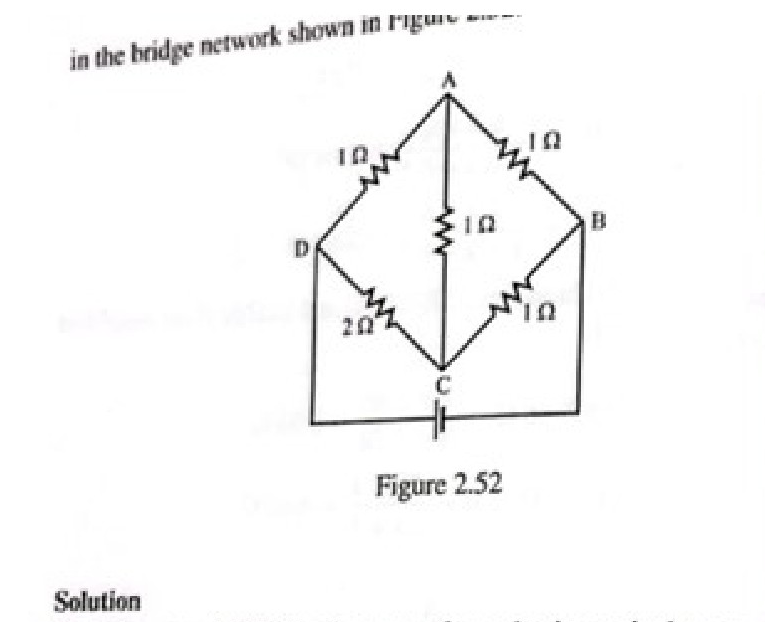
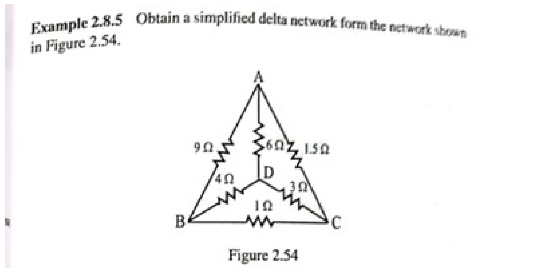
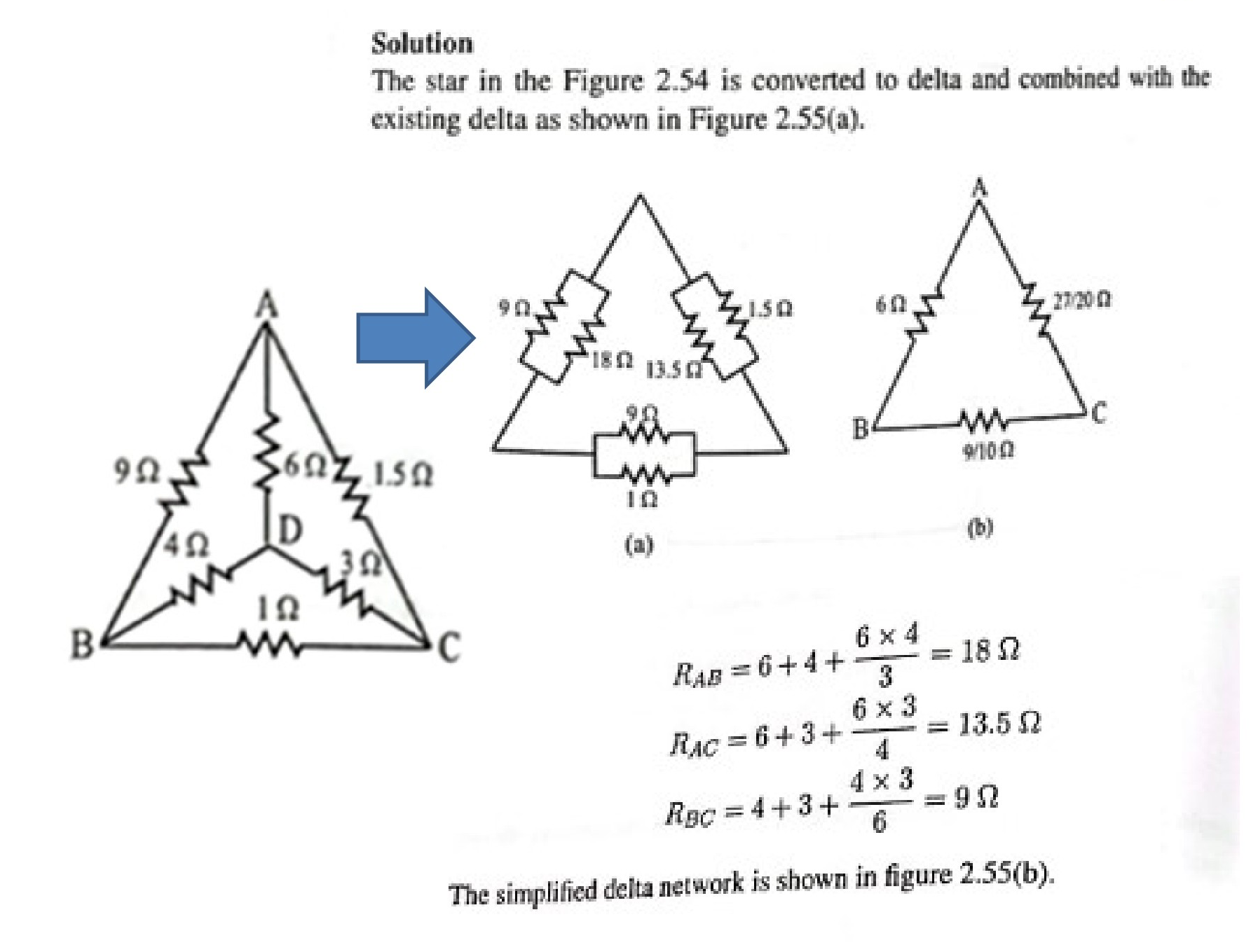
  55. equivalent resistance
  56. Star -- Delta Transformation
  57. Star -- Delta Transformation
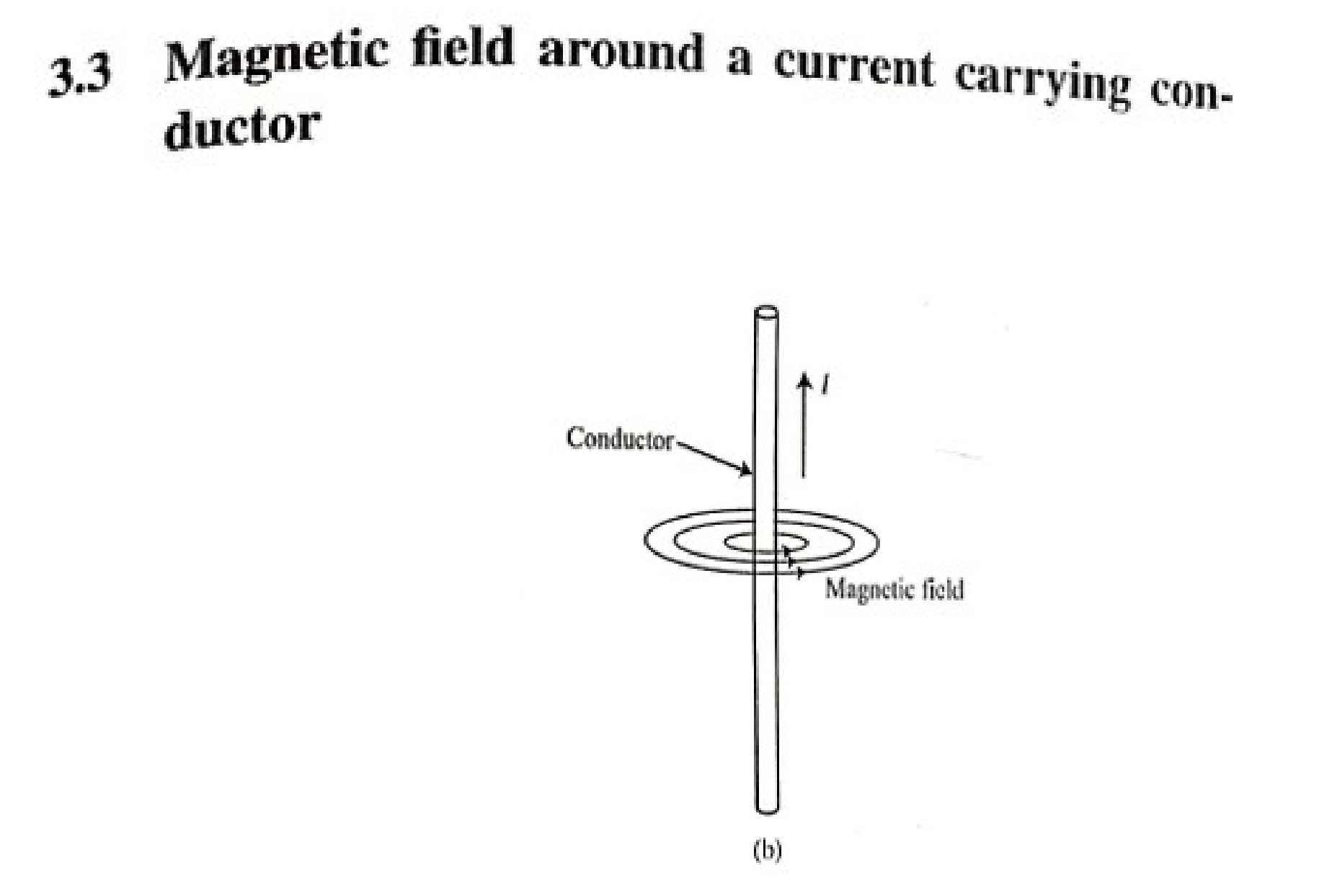
  58. Elementary concept of magnatic circuits ($2^{\text{nd}}$ half)
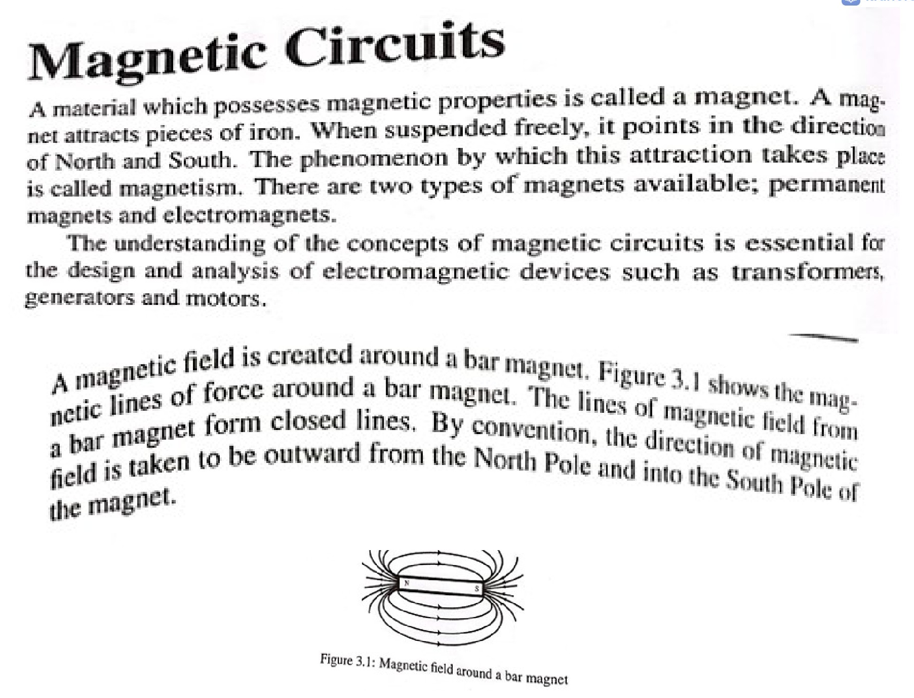
  59. Magnetic Circuits
  60. 3.4 Magnetic flux
  61. 3.5 Magnetic flux density
  62. 3.6 Magneto motive force
  63. 3.7 Magnetic field intensity
  64. 3.8 Permeability
  65. 3.9 Relative permeability
  66. 3.10 Reluctance
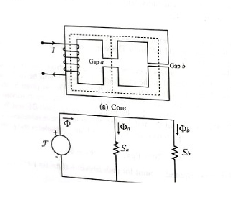
  67. 3.11 Comparison of electric and magnetic circuits
  68. Differences between electric and magnetic circuits
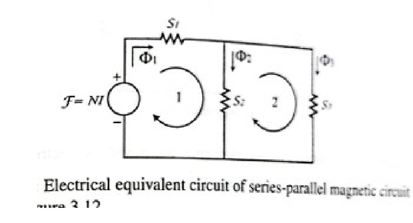
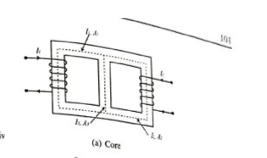
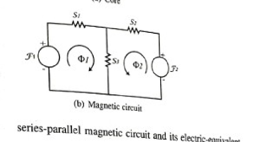
  69. 3.17.1 Series magnetic circuit
  70. why this air gap?
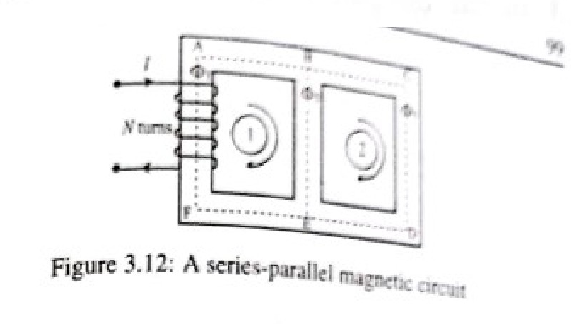
  71. 3.17.2 Series-parallel magnetic circuits
Text size18

Page 1 of 185

[Non-content page]


Page 2 of 185

[Non-content page]


Page 3 of 185

[Non-content page]


Page 4 of 185

Syllabus : Elementary concepts of DC electric circuits : ((1 st half))

  • Basics-- Capacitors & Inductors: V-I relations and Energy stored. Current and Voltage Division Rule - Relative potential
  • Ohms Law and Kirchhoff's laws - numerical problems.
  • Star-delta conversion (resistive networks only - derivation not required) - numerical problems.

Page 5 of 185

Resistor

An illustrated cutaway of a carbon composition resistor showing internal structure and color code bands

  • A resistor is a passive two-terminal electrical component that restricts or regulates the flow of electric current in a circuit.
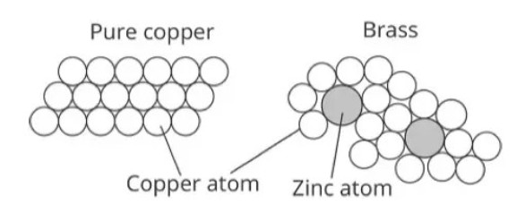
  • this Resistance resists current through atomic collisions
  • Unit of Measurement: Resistance is measured in ohms ( extOmega\text{ extOmega}). Ohm's Law: A resistor's behavior is defined by the formula (R=V/IR = V/I), where RR is resistance, VV is voltage, and II is current.

Diagram comparing pure copper crystal structure with brass alloy structure containing copper and zinc atoms


Page 6 of 185

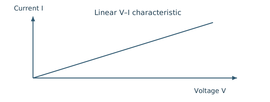
V-I characteristics

V-I characteristics graph showing a linear relationship between voltage and current


Page 7 of 185

Capacitor

Capacitance is the ability of a circuit element to store electric charge. Two conductors separated by an insulating material (the dielectric) form a capacitor.

If QQ is the stored charge in coulombs and VV is the applied voltage,

Q=CV,C=QV.Q=CV,\qquad C=\frac{Q}{V}.

The unit of capacitance is the farad (F).

For a capacitor charged from zero to VV, the average charging voltage is V/2V/2. The stored energy is

E=12QV=12CV2.E=\frac{1}{2}QV=\frac{1}{2}CV^2.


Page 8 of 185

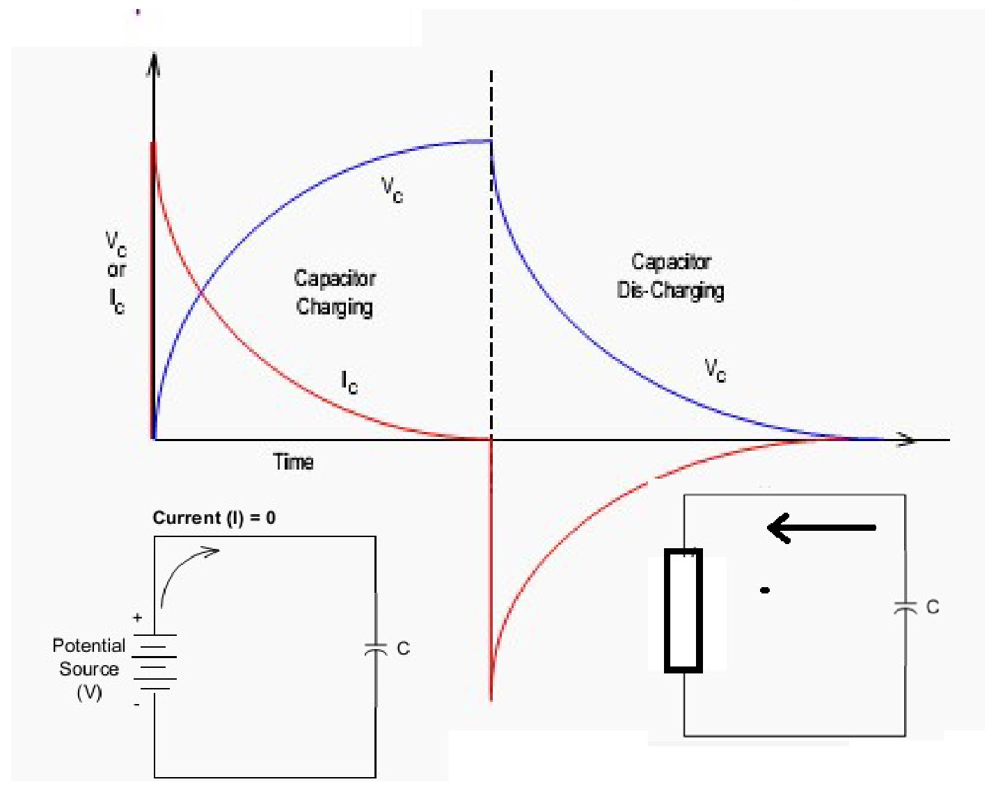
V-I relation of capacitor

V-I relation of capacitor during charging and discharging


Page 9 of 185

INDUCTANCE

Types of inductors: air core, iron core, ferrite core, and variable core

  • Inductance is the property of an electrical circuit that <font color="red">resists changes in current</font>. The SI unit of inductance is <font color="red">henry (H)</font>.
  • It <font color="red">stores energy in a form of magnetic field when current flows through it</font>.

v−iv - i relationship in an inductance is given by v=Ldidtv = L \frac{di}{dt}


Page 10 of 185

V-I characteristic

V-I characteristic and inductor response graph with circuit diagrams

Inductors are a Short circuit to DC Current


Page 11 of 185

  • Switching ON)
  • At t=0 (The instant the switch closes): The inductor acts like an Open Circuit.
    • Voltage (VV): Is at its maximum (equal to the battery voltage).
    • Current (II): Is exactly zero.
  • Steady state
    • Current (II): The current reaches its maximum value
    • voltage across an ideal inductor drops to 0 Volts.
  • Load is on
  • Current (II): Is gradually reduce to zero
  • Voltage (VV): Is at its maximum reversed (negative)

Page 12 of 185

[Non-content page]


Page 13 of 185

Inductor (L)

  • An inductor stores energy in a magnetic field created by current flowing through a coil of wire.
  • The energy stored in an inductor's magnetic field is given by:

WL=12Li2W_L = \frac{1}{2}Li^2


Page 14 of 185

constant Voltage source

  • A device that maintains a constant voltage; and the output current changes depending on the connected load resistance.
  • Internal Resistance: Has a very low (ideally zero) internal resistance.
  • Behavior on Short Circuit: Tries to supply infinite current, which can damage the device or blow a fuse.
  • Behavior on Open Circuit: Outputs its rated voltage with zero current flow.

Page 15 of 185

Behavior on load

Circuit diagram showing a resistor connected across a constant voltage source battery

Resistor (R)

I vary

V constant

constant Voltage source

Battery


Page 16 of 185

Behavior on Short Circuit

Circuit diagram showing a short circuit with a battery, fuse, and switch, with a lightning bolt pointing to the fuse.


Page 17 of 185

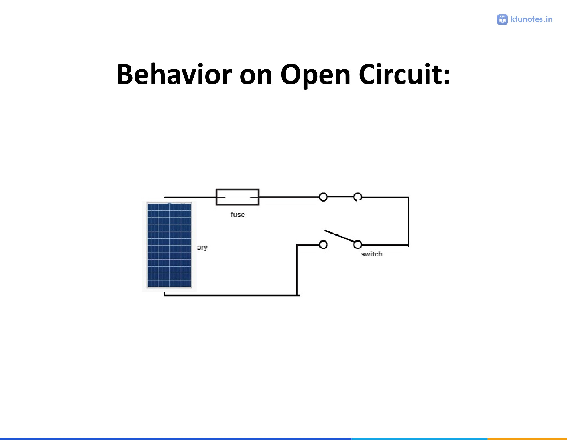
Behavior on Open Circuit:

Circuit diagram showing a battery, a fuse, and two switches connected in series


Page 18 of 185

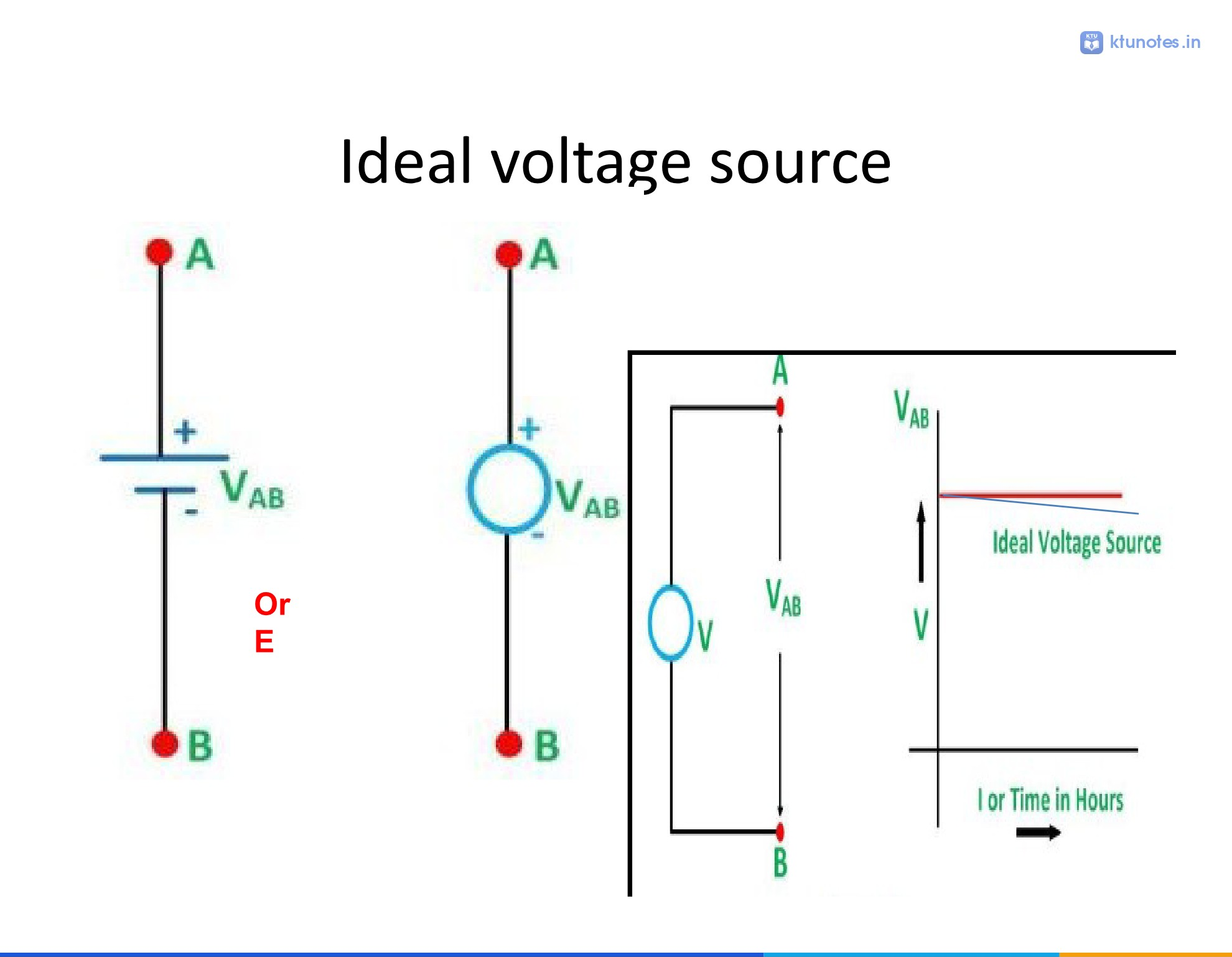
Ideal voltage source

Two alternative circuit symbols for an ideal voltage source between terminals A and B

Or E

Circuit diagram and V-I or V-time characteristic curve for an ideal voltage source


Page 19 of 185

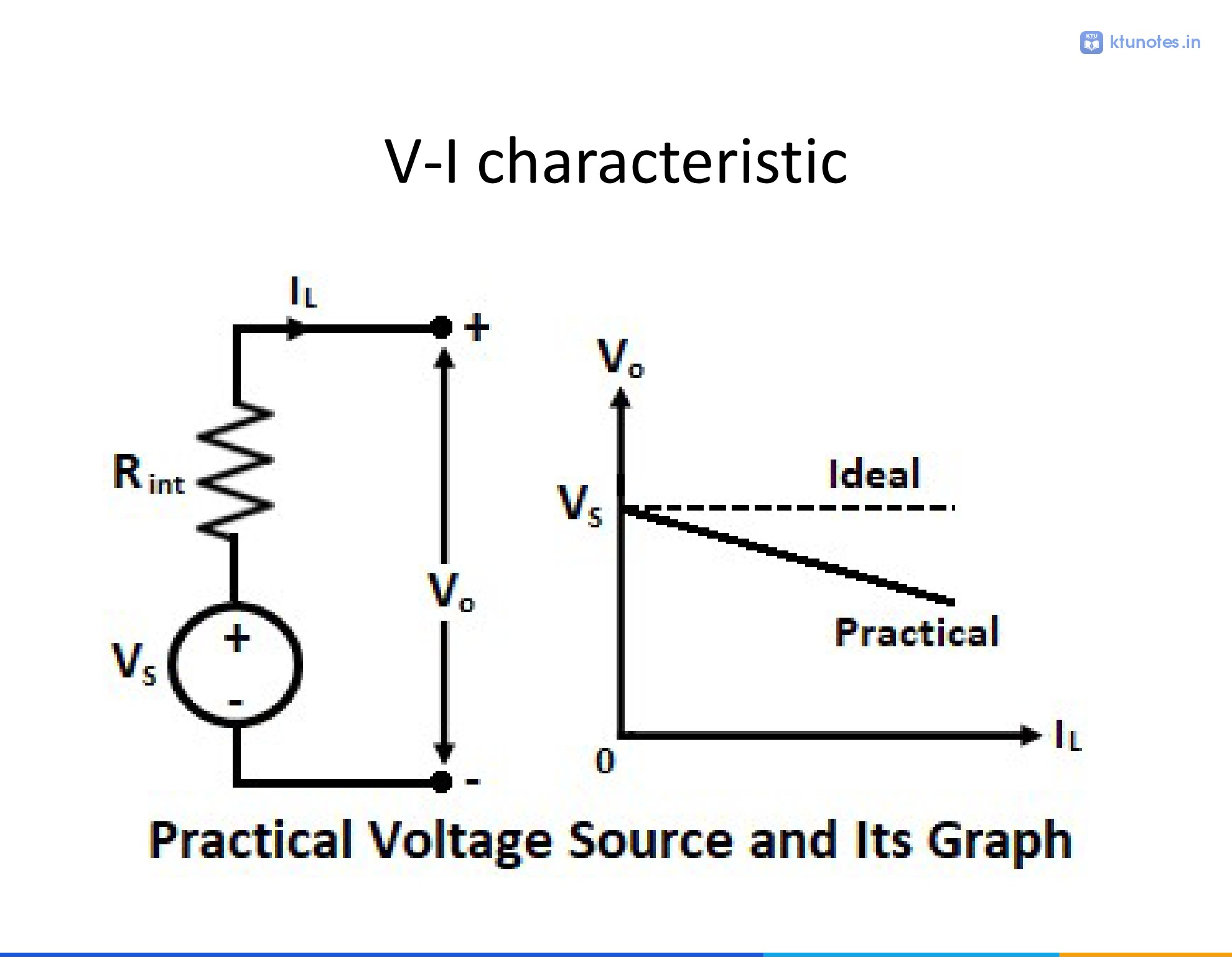
V-I characteristic

Circuit diagram of a practical voltage source with internal resistance R_int and a V-I characteristic graph showing ideal and practical curves.

Practical Voltage Source and Its Graph


Page 20 of 185

Constant Current Source

  • Definition: A device that maintains a constant current; the output voltage changes depending on the connected load resistance.
  • Internal Resistance: Has a very high (ideally infinite) internal resistance.
  • Behavior on Short Circuit: Safely delivers its rated current at near-zero voltage.
  • Behavior on Open Circuit: Tries to drive voltage to its maximum limit to force current

Page 21 of 185

Behavior on Open Circuit:

Circuit diagram showing a solar panel or battery connected in series with a fuse, an open switch, and another open switch.


Page 22 of 185

[Non-content page]


Page 23 of 185

[Non-content page]


Page 24 of 185

V-I characteristic

Circuit diagram of a current source in parallel with a resistor

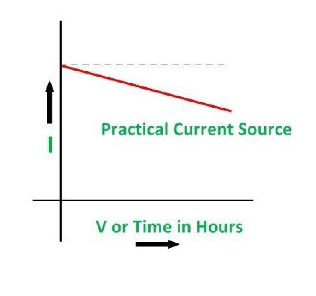
Graph showing the V-I characteristic of a practical current source


Page 25 of 185

Circuit diagram with a resistor connected to a DC power source or solar panel


Page 26 of 185

SI units of electrical quantities

QuantityUnitSymbol
CurrentAmpereA
VoltageVoltV
PowerWattW
EnergyJouleJ
ResistanceOhmΩ

Page 27 of 185

Series and parallel connection

ComponentSeries ConnectionParallel Connection
Resistors (RR)R1+R2 ...R_1 + R_2 \text{ ...} (Add)1R1+1R2 ...\frac{1}{R_1} + \frac{1}{R_2} \text{ ...} (Reciprocals)
Capacitors (CC)1C1+1C2 ...\frac{1}{C_1} + \frac{1}{C_2} \text{ ...} (Reciprocals)C1+C2 ...C_1 + C_2 \text{ ...} (Add)
Inductors (LL)L1+L2 ...L_1 + L_2 \text{ ...} (Add)1L1+1L2 ...\frac{1}{L_1} + \frac{1}{L_2} \text{ ...} (Reciprocals)

Page 28 of 185

Meaning of NETWORK & CIRCUIT

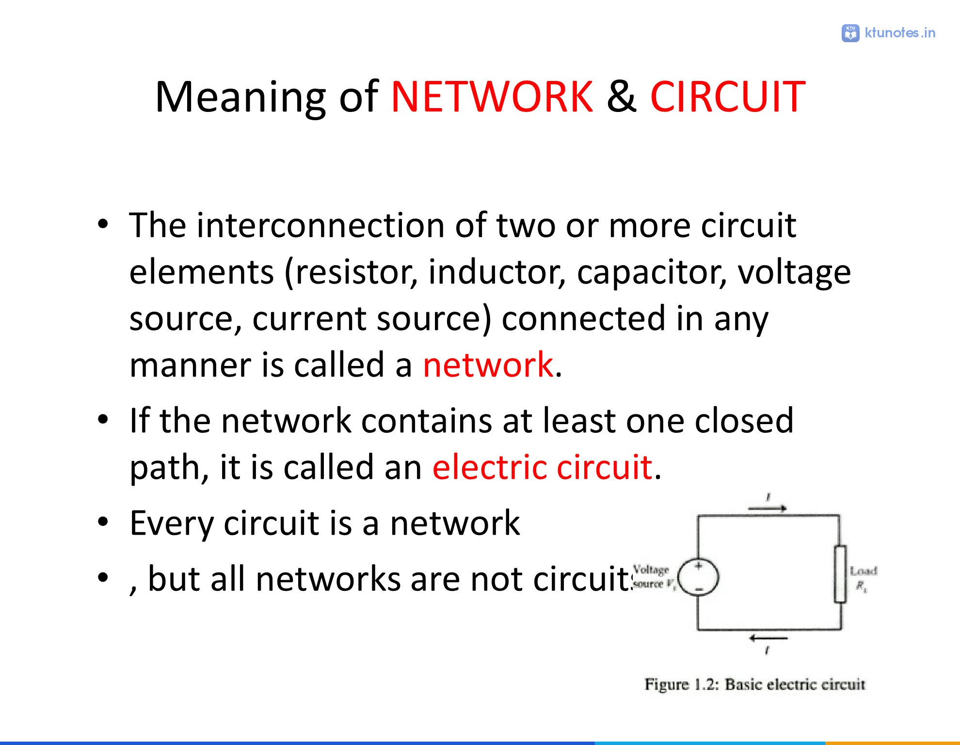
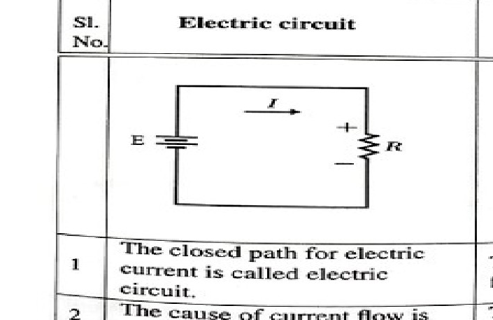
  • The interconnection of two or more circuit elements (resistor, inductor, capacitor, voltage source, current source) connected in any manner is called a network.
  • If the network contains at least one closed path, it is called an electric circuit.
  • Every circuit is a network
  • but all networks are not circuit.

Figure 1.2: Basic electric circuit showing a voltage source and load resistor in a closed loop

Figure 1.2: Basic electric circuit


Page 29 of 185

Ohm's law

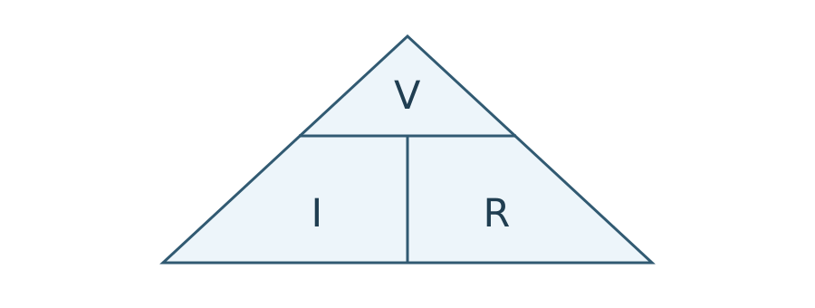
  • Ohm's law states that the current flowing through a conductor is directly proportional to the voltage across it and inversely proportional to its resistance, provided the temperature remains constant

Ohm's Law Triangle diagram showing the relationship between Voltage V, Current I, and Resistance R


Page 30 of 185

German physicist and mathematician Georg Simon Ohm

  • 16 March 1789 – 6 July 1854

Portrait of Georg Simon Ohm


Page 31 of 185

[Non-content page]


Page 32 of 185

American scientist Joseph Henry,

Portrait of American scientist Joseph Henry

The Henry Unit: One henry is defined as the inductance of a circuit where an induced voltage of one volt is produced by a current changing at a rate of one ampere per second.


Page 33 of 185

1.6 Resistances in series Based on ohms law

The circuit in which resistances are connected end to end so that there is only one path for current flow, is called a series circuit. In a series circuit,

  1. the same current flows through all resistances,
  2. there will be voltage drop across each resistance given by Ohm's law and
  3. the sum of the voltage drops is equal to the applied voltage.

Series circuit diagram with voltage source Vs, current I, and three series resistances R1, R2, R3 with voltage drops V1, V2, V3 respectively.


Page 34 of 185

3rd point

Series resistor circuit diagram with voltage source V_s, current I, resistors R1, R2, R3, and voltage drops V1, V2, V3

From Figure 1.7, VS=V1+V2+V3V_S = V_1 + V_2 + V_3

&= IR_1 + IR_2 + IR_3 \ &= I(R_1 + R_2 + R_3) \ &= IR \quad \text{where } R \text{ is the equivalent resistance.} \end{aligned}$ Then the equivalent resistance, $R = R_1 + R_2 + R_3$ ---

Page 35 of 185

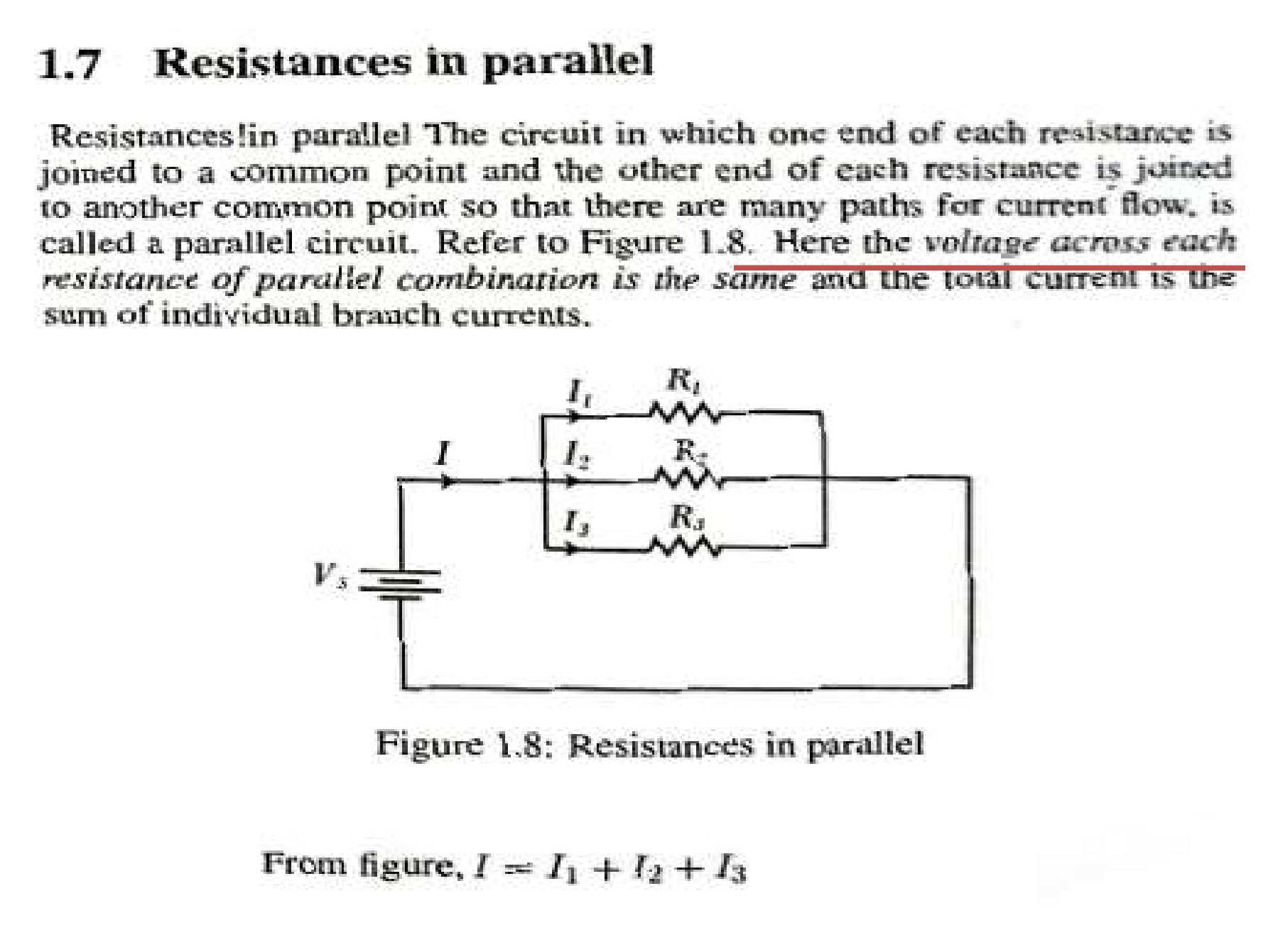
1.7 Resistances in parallel

Resistances in parallel The circuit in which one end of each resistance is joined to a common point and the other end of each resistance is joined to another common point so that there are many paths for current flow, is called a parallel circuit. Refer to Figure 1.8. Here the voltage across each resistance of parallel combination is the same and the total current is the sum of individual branch currents.

Circuit diagram showing three resistors in parallel connected to a voltage source

Figure 1.8: Resistances in parallel

From figure, I=I1+I2+I3I = I_1 + I_2 + I_3


Page 36 of 185

From figure, I=I1+I2+I3I = I_1 + I_2 + I_3

=VSR1+VSR2+VSR3= \frac{V_S}{R_1} + \frac{V_S}{R_2} + \frac{V_S}{R_3}

Let RR be the equivalent resistance of the circuit. Then I=VSRI = \frac{V_S}{R}

So, VSR=VS(1R1+1R2+1R3)\frac{V_S}{R} = V_S \left(\frac{1}{R_1} + \frac{1}{R_2} + \frac{1}{R_3}\right)

1R=1R1+1R2+1R3\frac{1}{R} = \frac{1}{R_1} + \frac{1}{R_2} + \frac{1}{R_3}

If resistances R1,R2,…RnR_1, R_2, \dots R_n are connected in parallel, then

G1R=1R1+1R2+⋯+1RnG \quad \frac{1}{R} = \frac{1}{R_1} + \frac{1}{R_2} + \dots + \frac{1}{R_n}

R=R1R2/R1+R2R = R_1R_2/R_1+R_2


Page 37 of 185

Application of ohms law

  1. voltage divider and current divider rules
  2. Source transformation rule

Page 38 of 185

Application 1

VOLTAGE DIVIDER AND CURRENT DIVIDER RULES

If current is not given in a circuit then voltage division rule can use

If voltage not given in a circuit then current division rule can use


Page 39 of 185

VOLTAGE DIVIDER RULE

Rule: The voltage across any resistor in a series network is equal to the ratio of its individual resistance to the total resistance of the series network, multiplied by the total voltage in the circuit..

Circuit diagram for voltage divider rule showing a voltage source V and two series resistors R1 and R2 with voltage drops V1 and V2

Figure 2 - Voltage Division Rule

v1v_1 = voltage across first resistor

VV = total voltage in the circuit

R1+R2R_1 + R_2 = total resistance

V1=VR1R1+R2V_1 = \frac{VR_1}{R_1 + R_2} V2=VR2R1+R2V_2 = \frac{VR_2}{R_1 + R_2}

Page 40 of 185

General Formula (N Resistors)

For a series connection of NN resistors, the voltage across any target resistor RxR_x is:

Vx=Vtotal⋅(RxRtotal)V_x = V_{\text{total}} \cdot \left(\frac{R_x}{R_{\text{total}}}\right)

where Rtotal=R1+R2+⋯+RNR_{\text{total}} = R_1 + R_2 + \dots + R_N.


Page 41 of 185

According to Ohm's law,

V1=IR1 and V2=IR2V_1 = IR_1 \text{ and } V_2 = IR_2

Let RR is the total resistance of the circuit, and it is given by,

R=R1+R2⋯(1)R = R_1 + R_2 \quad \cdots (1)

Also, from the circuit, we have,

V=IR=I(R1+R2)⋯(2)V = IR = I(R_1 + R_2) \quad \cdots (2)

But

I=V1R1=V2R2⋯(3)I = \frac{V_1}{R_1} = \frac{V_2}{R_2} \quad \cdots (3)

Therefore, from equations (2) & (3), we finally get,

V=V1R1(R1+R2)  ⟹  V⋅R1=V1⋅(R1+R2)  ⟹  V⋅R1R1+R2=V1V = \frac{V_1}{R_1}(R_1 + R_2) \implies V \cdot R_1 = V_1 \cdot (R_1 + R_2) \implies \frac{V \cdot R_1}{R_1 + R_2} = V_1

∴V1=VR1R1+R2⋯(4)\therefore V_1 = \frac{VR_1}{R_1 + R_2} \quad \cdots (4)

Similarly,

V=V2R2(R1+R2)V = \frac{V_2}{R_2}(R_1 + R_2)

∴V2=VR2R1+R2⋯(5)\therefore V_2 = \frac{VR_2}{R_1 + R_2} \quad \cdots (5)


Page 42 of 185

CURRENT DIVIDER RULE

Rule: The current in any branch is equal to the ratio of opposite branch resistance to the total resistance of the circuit multiplied by the total current in the circuit.

Current divider circuit diagram with two parallel resistors R1 and R2

I1=IR2R1+R2I_1 = \frac{IR_2}{R_1 + R_2} I2=IR1R1+R2I_2 = \frac{IR_1}{R_1 + R_2}

Page 43 of 185

The current II has been divided into I1I_1 and I2I_2 into two parallel branches

I1=VR1I2=VR2I_1 = \frac{V}{R_1} \hspace{5cm} I_2 = \frac{V}{R_2}

#x27; in math mode at position 134: …} \text{Parall}$̲$ $I = \frac{…" style="color:#cc0000"> ![Blue arrow pointing to the right](/notes/cse/s1/electrical/module-1/assets/page-043-image-1-code.svg) \hspace{1cm} \text{Parall}$ $I = \frac{V}{R_T}$ $= \frac{V(R_1 + R_2)}{R_1 R_2}$ But $V = I_1 R_1$. Substituting the value of $V$ in the above equation we get Current flow through R1 $\hspace{1cm} I = \frac{I_1 R_1 (R_1 + R_2)}{R_1 R_2} = \frac{I_1 (R_1 + R_2)}{R_2} \hspace{1cm} ![Blue arrow pointing to the right](/notes/cse/s1/electrical/module-1/assets/page-043-image-2-code.svg) \hspace{1cm} I_1 = \frac{I R_2}{R_1 + R_2}$ Current flow through R2 $\hspace{1cm} ![Blue arrow pointing to the right](/notes/cse/s1/electrical/module-1/assets/page-043-image-3-code.svg) \hspace{1cm} I_2 = \frac{I R_1}{R_1 + R_2}$ ---
Page 44 of 185

Important note

  • If current is not given in a circuit then voltage division rule can use
  • If voltage not given in a circuit then current division rule can use
  • If voltage and current available in a circuit use ohms law
  • Specifically asked in the question apply the rules

Page 45 of 185

Find voltage drop across each resistance.

Circuit diagram with a 6V voltage source and two series resistors of 200 ohm and 100 ohm.

Applying the voltage division rule voltage across 200 Ω200\,\Omega resistance we get

E1=Er1+r2r1E_1 = \frac{E}{r_1+r_2} r_1

E1=6200+100 X 200=4VE_1 = \frac{6}{200+100} \text{ X } 200 = 4\text{V}

Voltage across 100 Ω100\,\Omega resistance we get

E2=Er1+r2r2E_2 = \frac{E}{r_1+r_2} r_2

E2=6200+100 X 100=2VE_2 = \frac{6}{200+100} \text{ X } 100 = 2\text{V}


Page 46 of 185

Consider two resistors 20 Ω20\,\Omega and 40 Ω40\,\Omega are connected in a parallel with a current source of 20 A20\text{ A}. Find out the current flowing through each resistor in the parallel circuit.

Circuit diagram showing a parallel circuit with a current source of 20A and two resistors R1 (20 ohms) and R2 (40 ohms)

Applying the current division rule voltage across 20 Ω20\,\Omega resistance we get

I1=Ir1+r2r2I_1 = \frac{I}{r_1+r_2} r_2

I1=2020+40×40=13.33AI_1 = \frac{20}{20+40} \times 40 = 13.33\text{A}

Voltage across 40 Ω40\,\Omega resistance we get

I2=Ir1+r2r1I_2 = \frac{I}{r_1+r_2} r_1

I2=2020+40×20=6.67AI_2 = \frac{20}{20+40} \times 20 = 6.67\text{A}


Page 47 of 185

Example 1.11.1 A resistor of 5  Ω5\;\Omega is connected in series with a parallel combination of 6  Ω6\;\Omega and 3  Ω3\;\Omega. Find the supply current taken from a 35  V35\;\text{V} dc source.

Solution

Let RPR_P be the equivalent resistance of the parallel combination of 3  Ω3\;\Omega and 6  Ω6\;\Omega.

Then 1RP=13+16=36\dfrac{1}{R_P} = \dfrac{1}{3} + \dfrac{1}{6} = \dfrac{3}{6}

Circuit diagram showing a parallel combination of 3 ohm and 6 ohm resistors in series with a 5 ohm resistor, connected across a 35 V source.

Therefore, RP=2  ΩR_P = 2\;\Omega

Total resistance in the circuit, R=RP+5=2+5=7  ΩR = R_P + 5 = 2 + 5 = 7\;\Omega

Supply current, I=VR=357=5  AI = \dfrac{V}{R} = \dfrac{35}{7} = 5\;\text{A}


Page 48 of 185

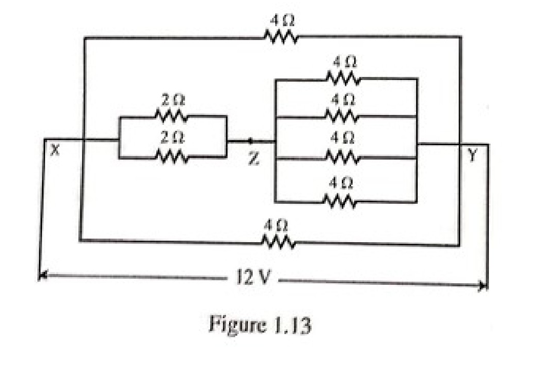
Example 1.11.2 Find the total resistance of the circuit across the terminals X and Y. Also find the power consumed by the circuit if a 12 V12\text{ V} battery is connected across XY.

Circuit diagram with resistors connected between terminals X and Y

Figure 1.13

Solution

R_{XZ} &= \frac{2 \times 2}{2 + 2} = 1\text{ }\Omega\\ \frac{1}{R_{ZY}} &= \frac{1}{4} + \frac{1}{4} + \frac{1}{4} + \frac{1}{4} = \frac{4}{4} = 1 \end{aligned}$ So, $R_{ZY} = 1\text{ }\Omega$ ![Simplified circuit diagram](/notes/cse/s1/electrical/module-1/assets/page-048-image-2-source.png) ---

Page 49 of 185

RXZ+RZY=1+1=2 ΩR_{XZ} + R_{ZY} = 1 + 1 = 2\, \Omega 1RXY=14+12+14=1\frac{1}{R_{XY}} = \frac{1}{4} + \frac{1}{2} + \frac{1}{4} = 1

Therefore, equivalent resistance, RXY=1 ΩR_{XY} = 1\, \Omega

Total current in the circuit, I=VRXY=121=12 AI = \frac{V}{R_{XY}} = \frac{12}{1} = 12\text{ A}

Power consumed =VI=12×12=144 W= VI = 12 \times 12 = 144\text{ W}


Page 50 of 185

Example 1.11.3 Three resistors 10 Ω10\ \Omega, 20 Ω20\ \Omega and 30 Ω30\ \Omega are connected in series across a 100 V100\text{ V} supply. Find the voltage across each resistor.

Solution

Circuit diagram of three resistors connected in series with a voltage source V = 100 V

Figure 1.15

Let RSR_S be the equivalent series resistance

RS=10+20+30=60 ΩR_S = 10 + 20 + 30 = 60\ \Omega

I=VRS=10060=1.666 AI = \frac{V}{R_S} = \frac{100}{60} = 1.666\text{ A}

Voltage drop across 10 Ω10\ \Omega, V1=1.666×10=16.66 VV_1 = 1.666 \times 10 = 16.66\text{ V}

Voltage drop across 20 Ω20\ \Omega, V2=1.666×20=33.33 VV_2 = 1.666 \times 20 = 33.33\text{ V}

Voltage drop across 30 Ω30\ \Omega, V3=1.666×30=50 VV_3 = 1.666 \times 30 = 50\text{ V}


Page 51 of 185

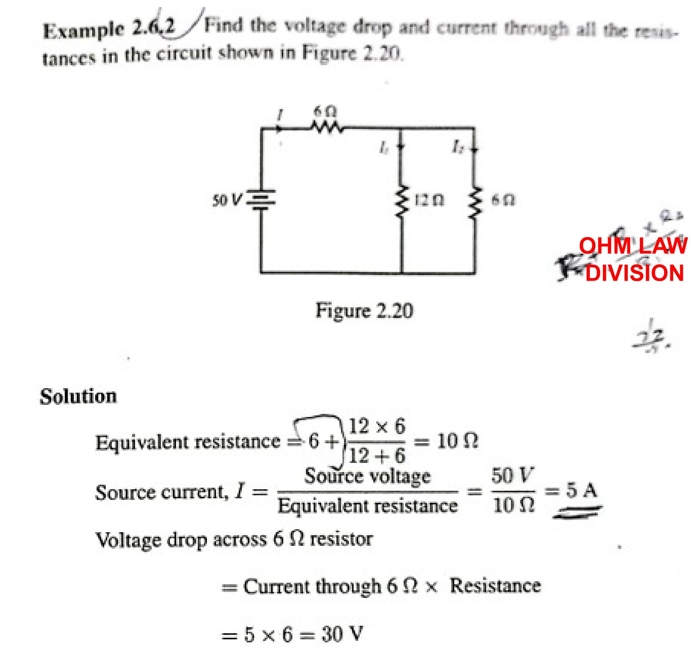
Example 2.6.2 Find the voltage drop and current through all the resistances in the circuit shown in Figure 2.20.

Circuit diagram with a 50V DC source, a 6 ohm series resistor, and two parallel branches with 12 ohm and 6 ohm resistors.

Figure 2.20

Solution

Equivalent resistance=6+12×612+6=10  Ω\text{Equivalent resistance} = 6 + \frac{12 \times 6}{12 + 6} = 10\;\Omega

Source current,I=Source voltageEquivalent resistance=50  V10  Ω=5  A\text{Source current}, I = \frac{\text{Source voltage}}{\text{Equivalent resistance}} = \frac{50\;\text{V}}{10\;\Omega} = 5\;\text{A}

Voltage drop across 6  Ω6\;\Omega resistor

=Current through 6  Ω×Resistance= \text{Current through } 6\;\Omega \times \text{Resistance}

=5×6=30  V= 5 \times 6 = 30\;\text{V}


Page 52 of 185

Using current divider rule, current through 12 Ω12\ \Omega resistor =I1= I_1

=5×612+6=53 A\quad = 5 \times \frac{6}{12 + 6} = \frac{5}{3}\text{ A}

By Kirchhoff's current law, I=I1+I2I = I_1 + I_2

Therefore, I2=I−I1=5−53=103 AI_2 = I - I_1 = 5 - \frac{5}{3} = \frac{10}{3}\text{ A}

Voltage drop across 12 Ω=I1×12=53×12=20 V12\ \Omega = I_1 \times 12 = \frac{5}{3} \times 12 = 20\text{ V}

Voltage drop across 6 Ω=I2×6=103×6=20 V6\ \Omega = I_2 \times 6 = \frac{10}{3} \times 6 = 20\text{ V}

The voltage across 6 Ω6\ \Omega and 12 Ω12\ \Omega resistors are the same because they are connected in parallel.


Page 53 of 185

Application 2

  • Ohms law

Page 54 of 185

Source transformation rule

Voltage source to current source

Diagram showing voltage source to current source transformation

Figure 2.5: Voltage source to current source transformation

A voltage source VsV_s in series with resistance RR can be transformed into a current source IsI_s in parallel with resistance RR where Is=VsRI_s = \frac{V_s}{R}


Page 55 of 185

Current source to voltage source

Current source to voltage source transformation diagram

Figure 2.6: Current source to voltage source transformation

Similarly, a current source ISI_S in parallel with a resistance RR can be transformed into a voltage VSV_S series with a resistance RR where VS=ISRV_S = I_S R


Page 56 of 185

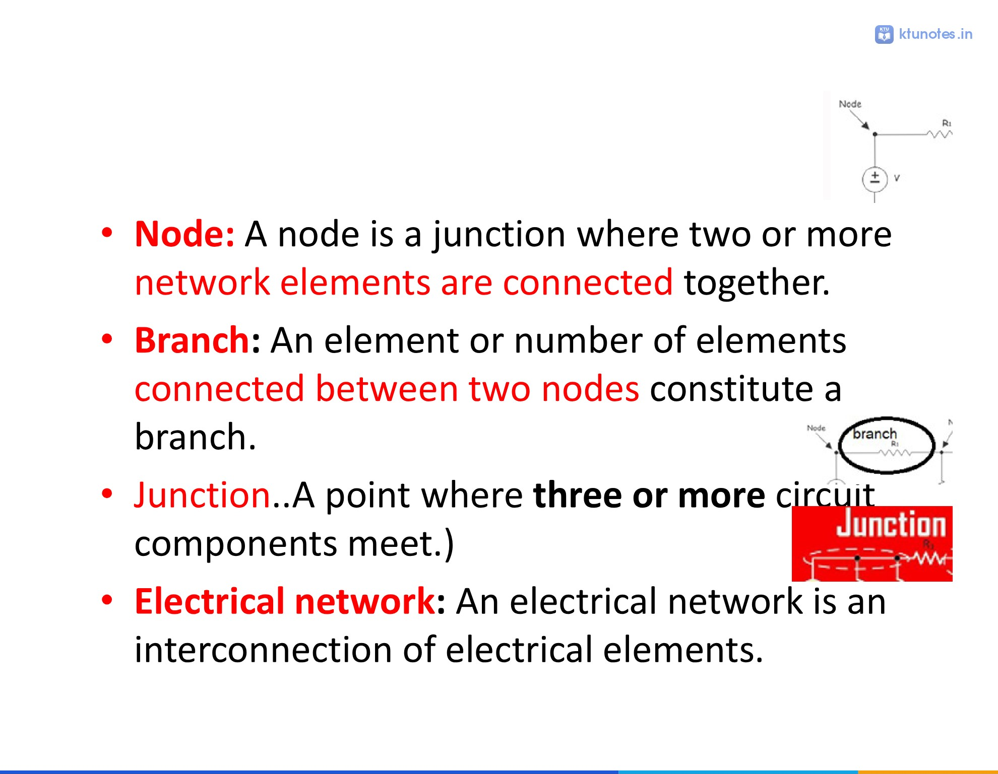
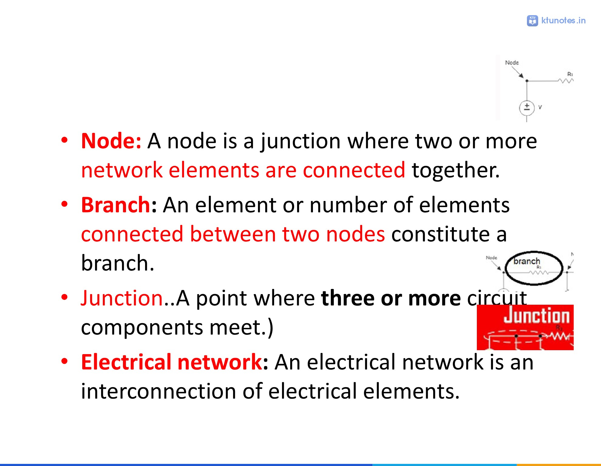
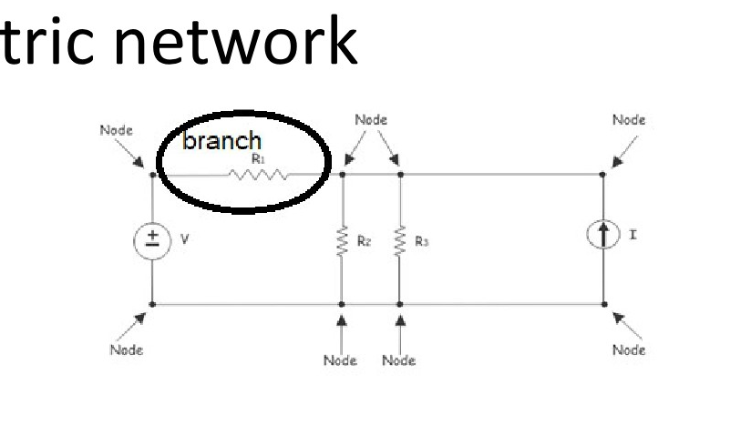
  • Node: A node is a junction where two or more network elements are connected together.

Node diagram

  • Branch: An element or number of elements connected between two nodes constitute a branch.

Branch diagram

  • Junction: A point where three or more circuit components meet.

Junction diagram

  • Electrical network: An electrical network is an interconnection of electrical elements.

Page 57 of 185

Important points

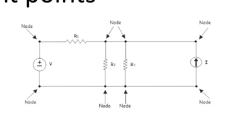
  • NODE
  • JUNCTION
  • BRANCH
  • LOOP
  • MESH
  • Electric network

Circuit diagram illustrating nodes

Circuit diagram illustrating branch


Page 58 of 185

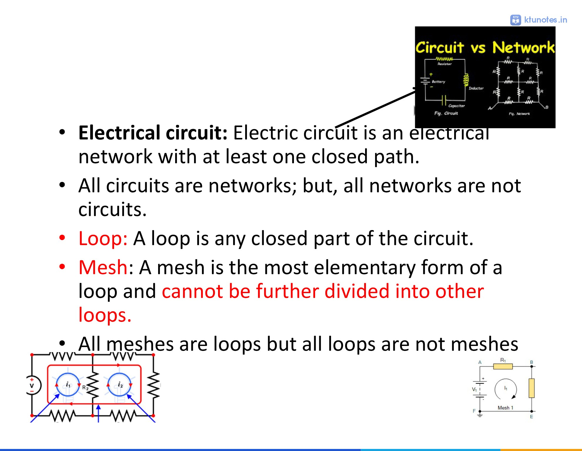
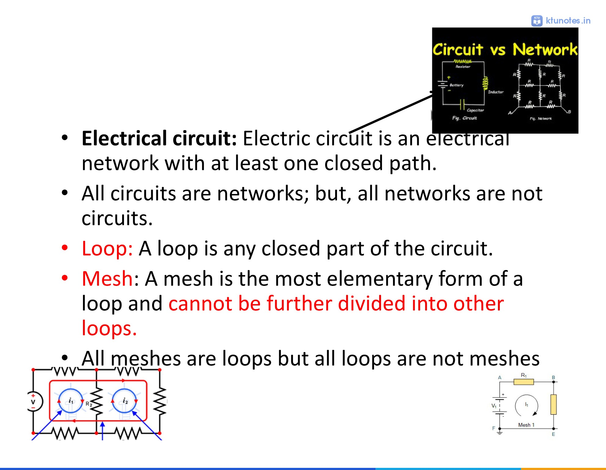
Circuit vs Network

Circuit vs Network comparison diagram showing a simple circuit with a battery, resistor, and capacitor, alongside a complex network of resistors.

  • Electrical circuit: Electric circuit is an electrical network with at least one closed path.
  • All circuits are networks; but, all networks are not circuits.
  • Loop: A loop is any closed part of the circuit.
  • Mesh: A mesh is the most elementary form of a loop and cannot be further divided into other loops.
  • All meshes are loops but all loops are not meshes

Two-mesh circuit diagram illustrating loop currents i1 and i2.

Single mesh circuit labeled Mesh 1 with current i1, voltage source V1, and resistor R1.


Page 59 of 185

  1. Absolute (Node) Potential (VAV_A): The voltage at Node A measured relative to the reference node (Ground, which is assumed to be 0 V0\text{ V}).

  2. Relative Potential (VABV_{AB}): The voltage at Node A relative to Node B.

The Formula:

VAB=VA−VBV_{AB} = V_A - V_B


Page 60 of 185

Relative potential

  • Relative potential (or potential difference) is the voltage of one point in a circuit measured with respect to another point, rather than to ground.

Circuit diagram illustrating absolute and relative potential with nodes A, B, C, D, resistors, a voltage source, and ground.


Page 61 of 185

Circuit diagram illustrating electrical concepts including Nodes, Branches, and Loops


Page 62 of 185

A branch is a single path containing a circuit component connected between two nodes

Circuit diagram illustrating branches with resistors and a voltage source


Page 63 of 185

Finding Loops in a Circuit

Circuit diagram illustrating loops with resistors, a voltage source, and mesh currents i1 and i2


Page 64 of 185

Mesh

  • A closed loop that doesn't contain any other loop within it is referred to as a mesh. In other words, any path within a circuit that doesn't include any other path is considered a mesh

Circuit diagram illustrating Mesh 1 and Mesh 2


Page 65 of 185

The overall circuit depicted in fig-1 comprises 6 Nodes, 7 Branches, 3 Loops, and 2 Meshes, as illustrated in fig-6.

Circuit diagram illustrating nodes, branches, loops, and meshes


Page 66 of 185

Robert Kirchhoff was a German physicist and mathematician who contributed to the fundamental understanding of electrical circuits

  • Kirchhoff (1824–1887)

Portrait illustration of Robert Kirchhoff


Page 67 of 185

KIRCHHOFF'S VOLTAGE LAW

  • Kirchhoff's voltage law states that the algebraic sum of all voltages in a closed path in a circuit is always zero at all instants of time.
  • (Or) sum of potential drop is equal to sum of potential rises

Circuit diagram illustrating Kirchhoff's Voltage Law


Page 68 of 185

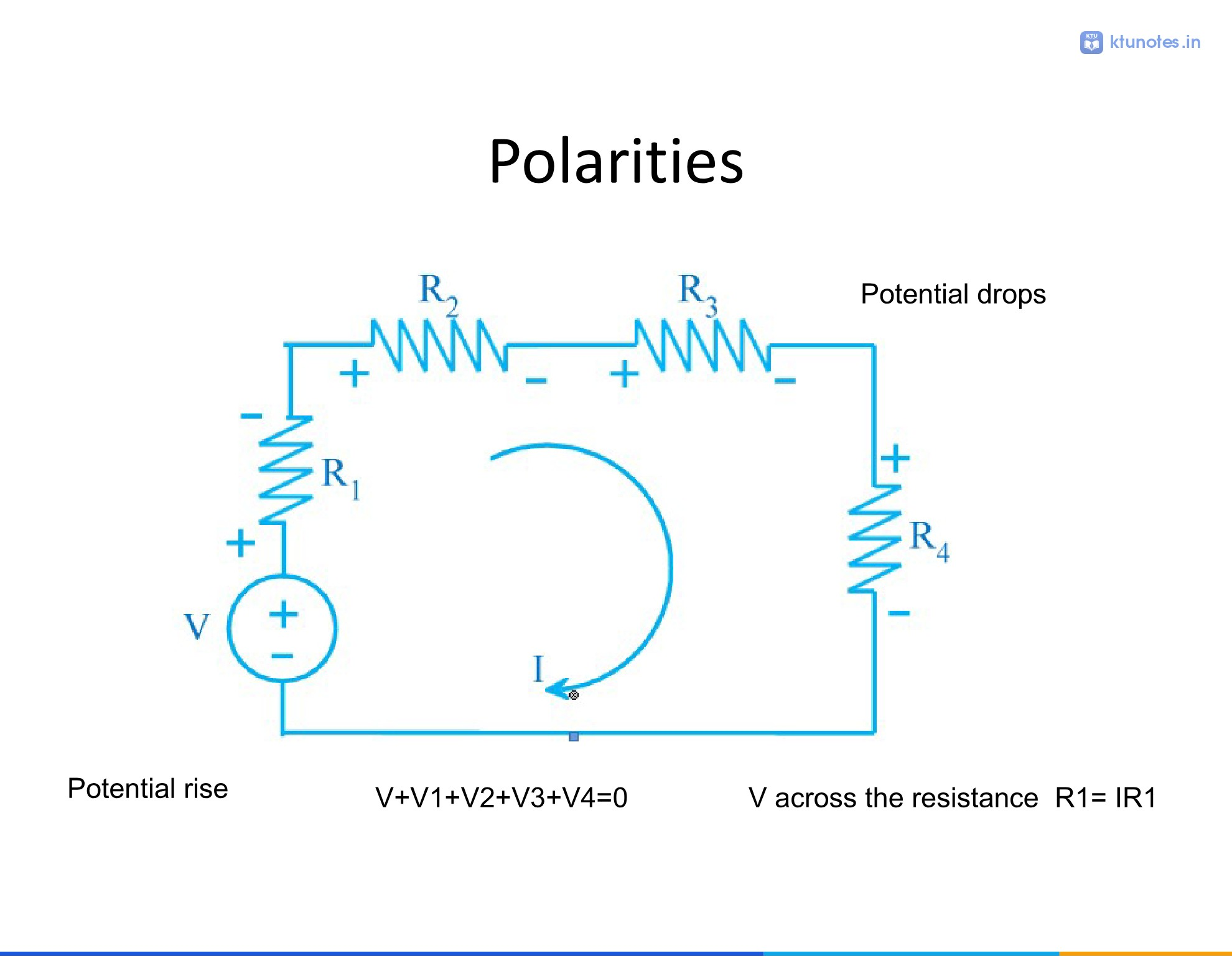
Polarities

Circuit diagram showing a closed loop with a voltage source V and four resistors R1, R2, R3, R4 with indicated polarities and current I

Potential rise

Potential drops

V+V1+V2+V3+V4=0V + V_1 + V_2 + V_3 + V_4 = 0

V across the resistance R1=IR1R_1 = IR_1


Page 69 of 185

Single loop electrical circuit with resistors and voltage sources

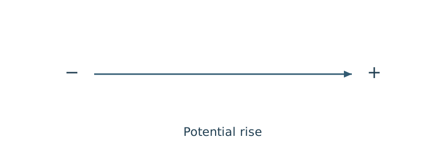
Potential rise icon showing transition from minus to plus

Potential rise

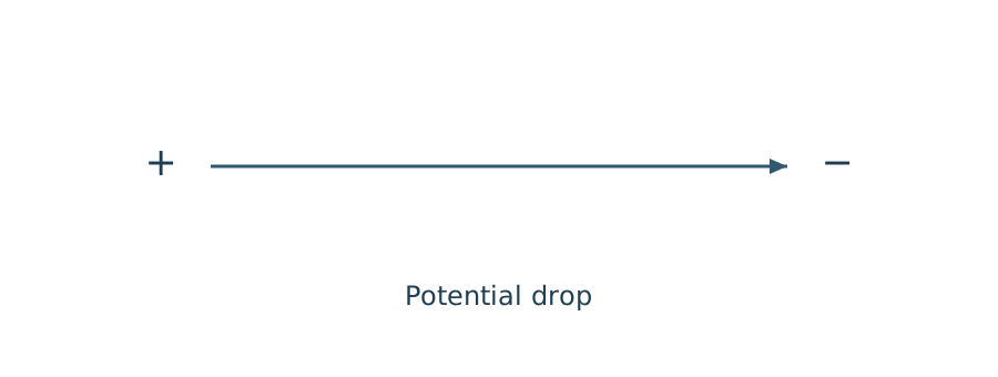
Potential drop icon showing transition from plus to minus

Potential drop

Current direction important(i1-i2) next loop (i2-i1) same direction Current direction important(i1+i2) next loop (i2+i1) opp direction

Voltage polarity very important Always start with voltage source for writing equations


Page 70 of 185

Sign convention for applying signs to the voltage polarities in our KVL equations

  • the loop, if the positive terminal is encountered before the negative terminal, the voltage is interpreted as positive in the KVL equation.
  • If the negative terminal is encountered first, the voltage is interpreted as negative in the KVL equation.

Page 71 of 185

Example kvl equation

Circuit diagram illustrating KVL with a voltage source V and resistors R1, R2, R3, and R4 in a single closed loop with clockwise current I.

Polarity convention inset box showing plus to minus gives negative (-ve) and minus to plus gives positive (+ve).

If we travel in clock-wise direction,

+V−IR1−IR2−IR3−IR4=0+V - IR_1 - IR_2 - IR_3 - IR_4 = 0


Page 72 of 185

1 mesh problems

KVL BASED PROBLEM

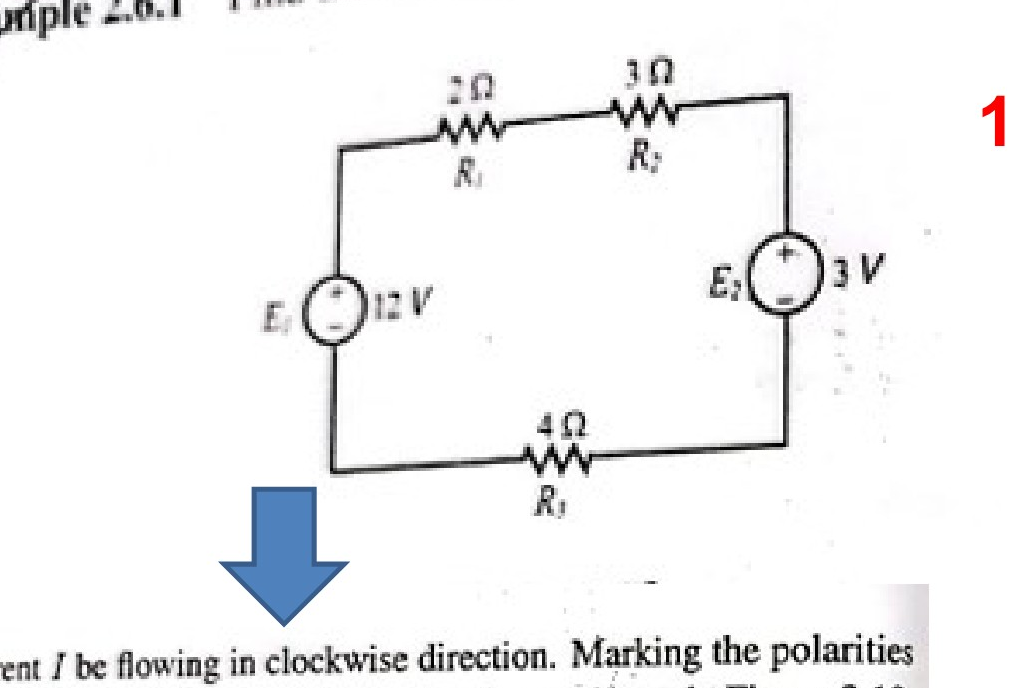
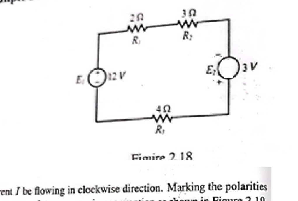
Example 2.6.1 Find the current in the circuit shown in Figure 2.

Circuit diagram with a single loop, three resistors, and two voltage sources

Solution

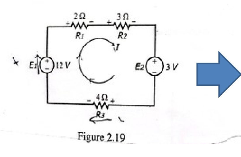
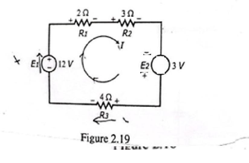
Let the current II be flowing in clockwise direction. Marking the polarities of voltages across resistors as per sign convention as shown in Figure 2.19.

Circuit diagram with clockwise current I and voltage polarities across components

Figure 2.19

Blue arrow pointing right

Applying KVL, we get,

E_1 - IR_1 - IR_2 - E_2 - IR_3 &= 0 \\ 12 - 2 \times I - 3 \times I - 3 - 4 \times I &= 0 \\ 9 - 9I &= 0 \\ \therefore \text{Current}, I &= 1\text{ A} end{aligned}$ ---

Page 73 of 185

KVL BASED PROBLEM

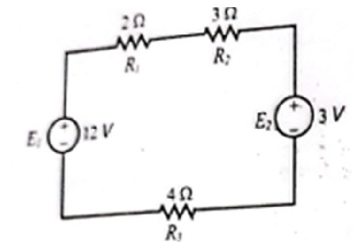
Example 2.6.1 Find the current in the circuit shown in Figure 2.18.

Circuit diagram with two voltage sources E1 (12 V) and E2 (3 V) and three resistors R1 (2 ohm), R2 (3 ohm), and R3 (4 ohm).

Figure 2.18

Solution

Let the current II be flowing in clockwise direction. Marking the polarities of voltages across resistors as per sign convention as shown in Figure 2.19.

Circuit diagram for Example 2.6.1 showing assumed clockwise loop current I and voltage polarities across all components.

Figure 2.19

Applying KVL, we get,

E_1 - IR_1 - IR_2 - E_2 - IR_3 &= 0 \ 12 - 2 \times I - 3 \times I - 3 - 4 \times I &= 0 \ 15 - 9I &= 0 \ 9I &= 15 \ I = \frac{15}{9} = \frac{5}{3} \text{ A} & hickapprox 1.67 \text{ A} end{aligned}$ ---

Page 74 of 185

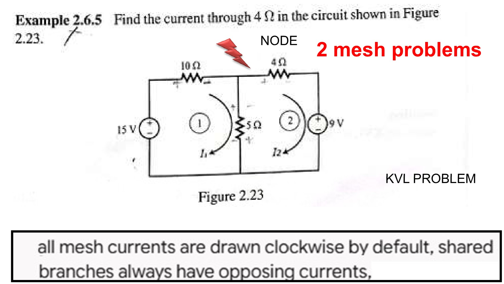
Example 2.6.5 Find the current through 4  Ω4 \; \Omega in the circuit shown in Figure 2.23.

NODE

2 mesh problems

Circuit diagram with two meshes, resistors, voltage sources, and mesh currents I1 and I2

KVL PROBLEM

all mesh currents are drawn clockwise by default, shared branches always have opposing currents,


Page 75 of 185

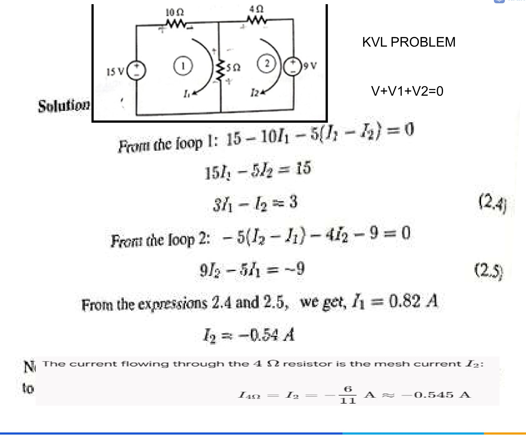
KVL PROBLEM

Electrical circuit diagram with two meshes

Solution

From the loop 1: 15−10I1−5(I1−I2)=015 - 10I_1 - 5(I_1 - I_2) = 0

15I1−5I2=1515I_1 - 5I_2 = 15

3I1−I2=3(2.4)3I_1 - I_2 = 3 \quad (2.4)

From the loop 2: −5(I2−I1)−4I2−9=0-5(I_2 - I_1) - 4I_2 - 9 = 0

9I2−5I1=−9(2.5)9I_2 - 5I_1 = -9 \quad (2.5)

From the expressions 2.4 and 2.5, we get, I1=0.82 AI_1 = 0.82 \text{ A}

I2=−0.54 AI_2 = -0.54 \text{ A}

Note: The current flowing through the 4 Ω4\,\Omega resistor is the mesh current I2I_2:

I4Ω=I2=−611 A≈−0.545 AI_{4\Omega} = I_2 = - \frac{6}{11} \text{ A} \approx -0.545 \text{ A}


Page 76 of 185

Solve the System of Simultaneous Equations

From Equation 1, express I2I_2 in terms of I1I_1:

I2=3I1−3I_2 = 3I_1 - 3

Substitute I2I_2 into Equation 2回忆:

5I_1 - 9(3I_1 - 3) &= 9 \ 5I_1 - 27I_1 + 27 &= 9 \ -22I_1 &= 9 - 27 \ -22I_1 &= -18 \ I_1 = \frac{-18}{-22} &= \frac{9}{11}\text{ A} \times 0.818\text{ A} Now, calculate $I_2$: $\begin{aligned} I_2 &= 3\binom{9}{11} - 3 \ I_2 &= \frac{27}{11} - \frac{33}{11} = -\frac{6}{11}\text{ A} \times -0.545\text{ A} Since the draft was actually very close, let's restore the precise standard markdown format without noise: Solve the System of Simultaneous Equations From **Equation 1**, express $I_2$ in terms of $I_1$: $I_2 = 3I_1 - 3$ Substitute $I_2$ into **Equation 2**: $\begin{aligned} 5I_1 - 9(3I_1 - 3) &= 9 \ 5I_1 - 27I_1 + 27 &= 9 \ -22I_1 &= 9 - 27 \ -22I_1 &= -18 \ I_1 = \frac{-18}{-22} &= \frac{9}{11}\text{ A} \times 0.818\text{ A} Now, calculate $I_2$: $\begin{aligned} I_2 &= 3\binom{9}{11} - 3 \ I_2 &= \frac{27}{11} - \frac{33}{11} = -\frac{6}{11}\text{ A} \times -0.545\text{ A} ---

Page 77 of 185

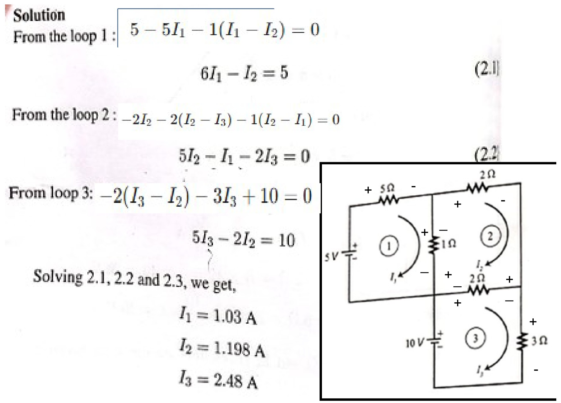
Example 2.6.3 Find the loop currents in the electric circuit shown in Figure 2.21.

3 mesh problems

KVL PROBLEM

Electric circuit diagram with 3 meshes and 3 mesh currents I1, I2, and I3


Page 78 of 185

Solution

From the loop 1 : 5−5I1−1(I1−I2)=05 - 5I_1 - 1(I_1 - I_2) = 0

6I_1 - I_2 = 5 \tag{2.1}

From the loop 2 : −2I2−2(I2−I3)−1(I2−I1)=0-2I_2 - 2(I_2 - I_3) - 1(I_2 - I_1) = 0

5I_2 - I_1 - 2I_3 = 0 \tag{2.2}

Circuit diagram with three loops and multiple resistors and voltage sources.

From loop 3 : −2(I3−I2)−3I3+10=0-2(I_3 - I_2) - 3I_3 + 10 = 0

5I_3 - 2I_2 = 10 \tag{2.3}

Solving 2.1, 2.2 and 2.3, we get,

I1=1.03 AI_1 = 1.03\text{ A}

I2=1.198 AI_2 = 1.198\text{ A}

I3=2.48 AI_3 = 2.48\text{ A}


Page 79 of 185

From (Eq. 1): I2=6I1−5I_2 = 6I_1 - 5

From (Eq. 3): 5I3=10+2I2=10+2(6I1−5)=10+12I1−10=12I1  ⟹  I3=2.4I15I_3 = 10 + 2I_2 = 10 + 2(6I_1 - 5) = 10 + 12I_1 - 10 = 12I_1 \implies I_3 = 2.4I_1

Substitute I2I_2 and I3I_3 into (Eq. 2):

I_1 - 5(6I_1 - 5) + 2(2.4I_1) &= 0 \\ I_1 - 30I_1 + 25 + 4.8I_1 &= 0 \\ -24.2I_1 &= -25 \end{aligned}$ $I_1 = \frac{25}{24.2} = \frac{125}{121} \approx 1.033\text{ A}$ Now, calculate $I_2$ and $I_3$: $I_2 = 6 \cdot \left(\frac{125}{121}\right) - 5 = \frac{750}{121} - \frac{605}{121} = \frac{145}{121} \approx 1.198\text{ A}$ $I_3 = 2.4 \cdot \left(\frac{125}{121}\right) = \frac{12}{5} \cdot \frac{125}{121} = \frac{300}{121} \approx 2.479\text{ A}$ ---

Page 80 of 185

Super mesh(note)

  • when a current source is located on the boundary shared by two meshes.
  • To solve this, we "remove" the shared current source branch and create a larger loop
  • Series Resistors: If a resistor is in series with the shared current source, it is "removed" along with the source
  • If a current source is on the outside of the circuit (not shared), you don't need a supermesh.

Page 81 of 185

points (Super mesh )

  • A supermesh is created in circuit analysis when a current source (independent or dependent) is shared between two adjacent meshes.
  • Temporarily remove the shared current source and any element connected strictly in series with it, leaving an open circuit.
  • Apply Kirchhoff's Voltage Law (KVL)

Page 82 of 185

current source is located on the boundary shared by two meshes.

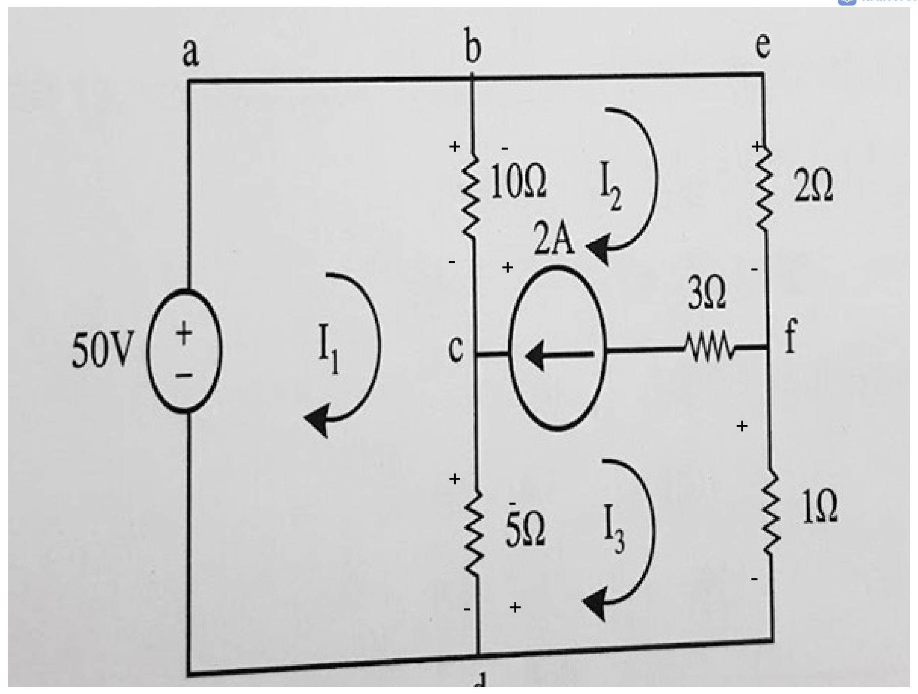
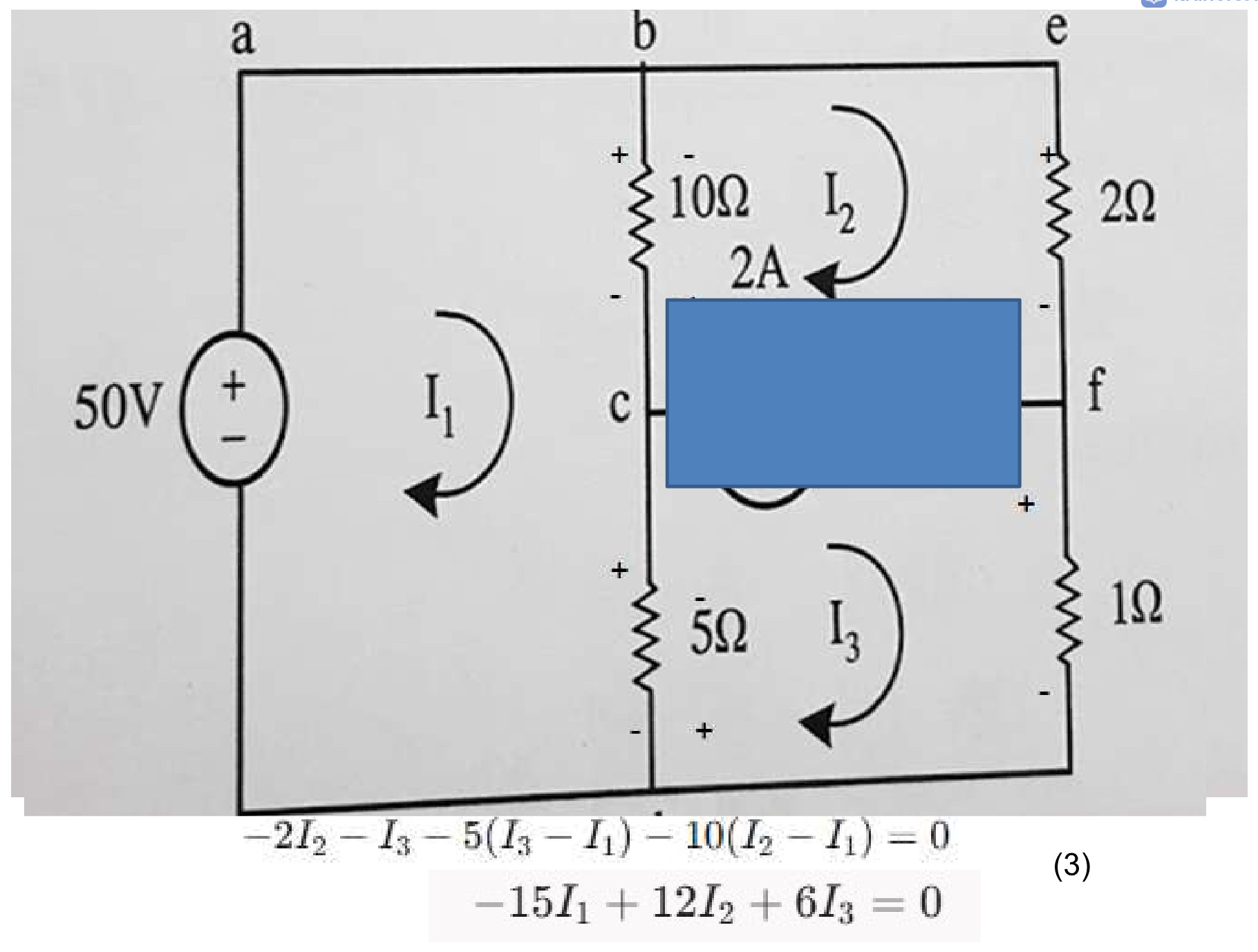
Example 1. Determine the current in the 5 Ω5\text{ }\Omega resistor in the network given in Fig.

Electrical network with meshes, resistors, a voltage source, and a current source


Page 83 of 185

Electrical circuit diagram with three mesh currents, voltage source, current source, and resistors


Page 84 of 185

50−10(I1−I2)−5(I1−I3)=050 - 10(I_1 - I_2) - 5(I_1 - I_3) = 0

(1)(1)

15I1−10I2−5I3=5015I_1 - 10I_2 - 5I_3 = 50

Step B: Write the Constraint Equation for the Supermesh

The 2 A2\text{ A} current source is in a branch shared by Mesh 2 and Mesh 3.

  • Current I2I_2 flows in the same direction as the source (right to left).
  • Current I3I_3 flows in the opposite direction (left to right).

Circuit diagram showing a supermesh with a 50V source, 10 ohm, 5 ohm, 2 ohm, 3 ohm, and 1 ohm resistors, and a 2A current source between mesh 2 and mesh 3.

I2−I3=2  ⟹  I2=I3+2−(Eq. 2)I_2 - I_3 = 2 \implies I_2 = I_3 + 2 - (\text{Eq. 2})


Page 85 of 185

Electrical circuit diagram with three mesh currents I1, I2, I3, resistors of 10 ohm, 2 ohm, 5 ohm, 1 ohm, a 50V voltage source, and a 2A current source with a blue overlay box.

−2I2−I3−5(I3−I1)−10(I2−I1)=0-2I_2 - I_3 - 5(I_3 - I_1) - 10(I_2 - I_1) = 0  −15I1+12I2+6I3=0(3)\ -15I_1 + 12I_2 + 6I_3 = 0 \quad (3)


Page 86 of 185

  1. Solve the System of Equations

Substitute I2=I3+2I_2 = I_3 + 2 from (Eq. 2) into (Eq. 1) and (Eq. 3):

From (Eq. 1):

3I1−2(I3+2)−I3=10  ⟹  3I1−3I3=14  ⟹  I1−I3=143 A3I_1 - 2(I_3 + 2) - I_3 = 10 \implies 3I_1 - 3I_3 = 14 \implies I_1 - I_3 = \frac{14}{3}\text{ A}

Interestingly, we don't need to go further because the question asks for the current in the 5 Ω5\text{ }\Omega resistor. Looking at the diagram, the net downward current in the 5 Ω5\text{ }\Omega resistor is exactly (I1−I3)(I_1 - I_3).

I5Ω=I1−I3=143 A≈4.67 AI_{5\Omega} = I_1 - I_3 = \frac{14}{3}\text{ A} \approx 4.67\text{ A}


Page 87 of 185

[Non-content page]


Page 88 of 185

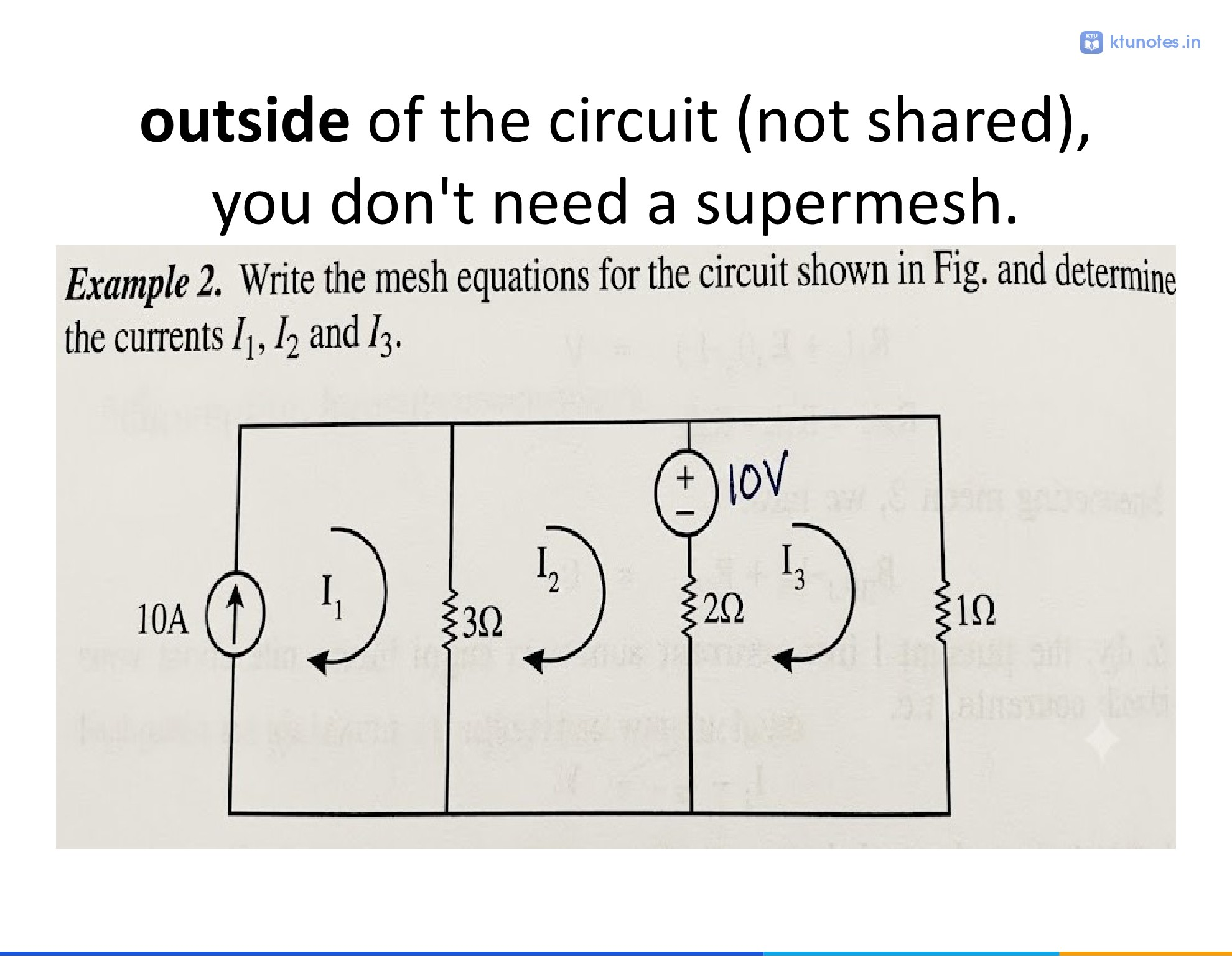
outside of the circuit (not shared), you don't need a supermesh.

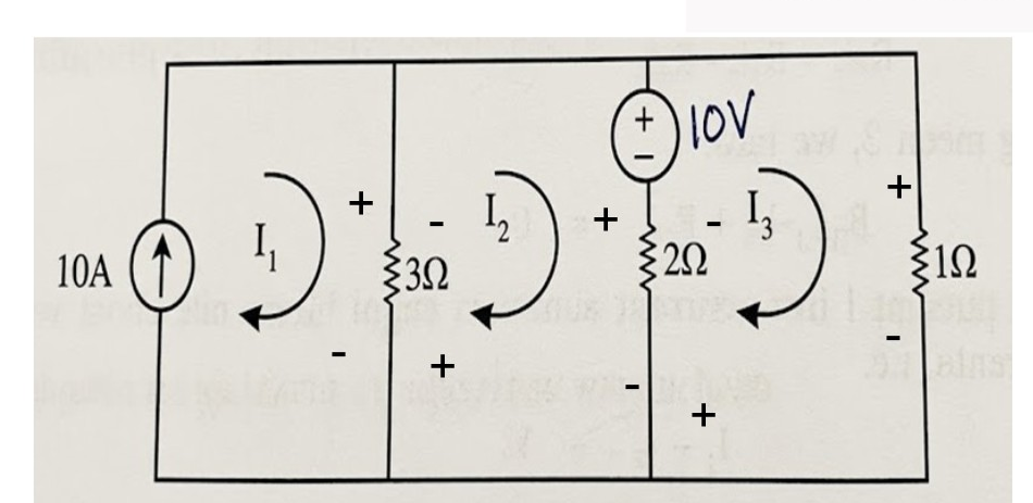
Example 2. Write the mesh equations for the circuit shown in Fig. and determine the currents I1I_1, I2I_2 and I3I_3.

Circuit diagram with three meshes containing a 10A current source, resistors of 3 ohms, 2 ohms, and 1 ohm, and a 10V voltage source.


Page 89 of 185

Summing the voltage drops to zero:

3(I2−I1)+10+2(I2−I3)=03(I_2 - I_1) + 10 + 2(I_2 - I_3) = 0

Substitute I1=10I_1 = 10:

3(I2−10)+10+2(I2−I3)=03(I_2 - 10) + 10 + 2(I_2 - I_3) = 0

3I2−30+10+2I2−2I3=03I_2 - 30 + 10 + 2I_2 - 2I_3 = 0

5I2−2I3=20— (Equation 1)5I_2 - 2I_3 = 20 \quad \text{--- (Equation 1)}

1⋅I3+2(I3−I2)−10=01 \cdot I_3 + 2(I_3 - I_2) - 10 = 0

−2I2+3I3=10— (Equation 2)-2I_2 + 3I_3 = 10 \quad \text{--- (Equation 2)}

Circuit diagram showing a mesh analysis problem with mesh currents I1, I2, I3, a 10A current source, a 3 ohm resistor, a 10V voltage source, a 2 ohm resistor, and a 1 ohm resistor.


Page 90 of 185

3. Solving the system of equations

From equation 2,

3I3=2I2+10,I3=2I2+103.3I_3=2I_2+10,\qquad I_3=\frac{2I_2+10}{3}.

Substitute into equation 1:

5I2−2(2I2+103)=20.5I_2-2\left(\frac{2I_2+10}{3}\right)=20.

Multiplying by 3 and simplifying,

15I2−4I2−20=60,11I2=80.15I_2-4I_2-20=60,\qquad 11I_2=80.

I2=8011 A≈7.27 A.I_2=\frac{80}{11}\,\mathrm{A}\approx7.27\,\mathrm{A}.

Then

I3=2(80/11)+103=27033=9011 A≈8.18 A.I_3=\frac{2(80/11)+10}{3}=\frac{270}{33}=\frac{90}{11}\,\mathrm{A}\approx8.18\,\mathrm{A}.

Final currents

I1=10 A,I2=8011 A,I3=9011 A.I_1=10\,\mathrm{A},\qquad I_2=\frac{80}{11}\,\mathrm{A},\qquad I_3=\frac{90}{11}\,\mathrm{A}.


Page 91 of 185

[Non-content page]


Page 92 of 185

Mesh current and matrix Representation

2.6.1 Matrix method of analysis

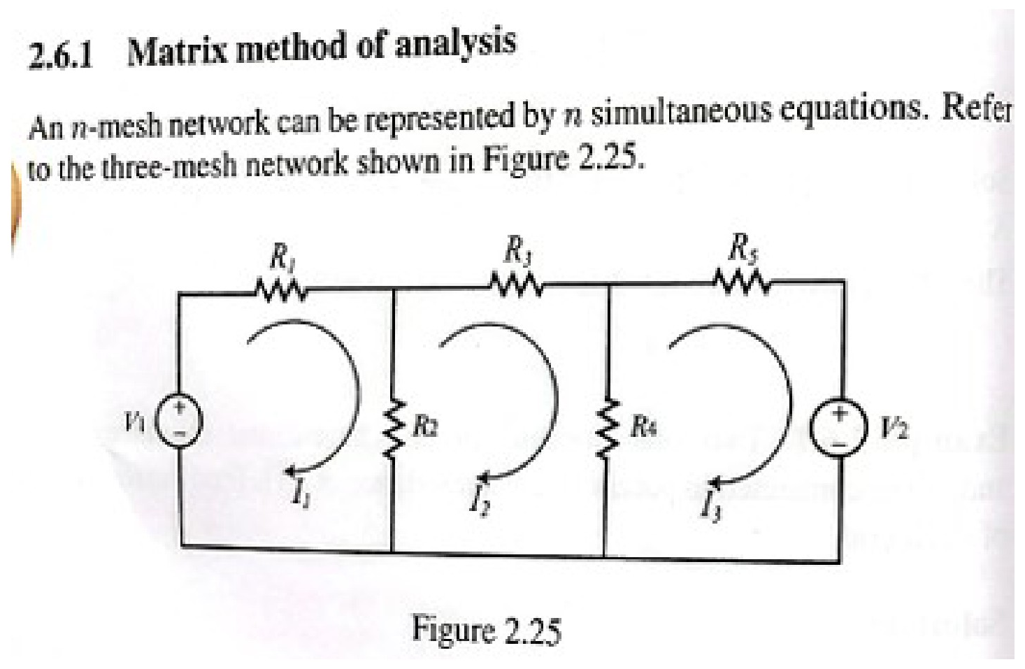
An nn-mesh network can be represented by nn simultaneous equations. Refer to the three-mesh network shown in Figure 2.25.

Three-mesh electrical network with resistors R1, R2, R3, R4, R5, voltage sources V1, V2, and mesh currents I1, I2, I3

Figure 2.25


Page 93 of 185

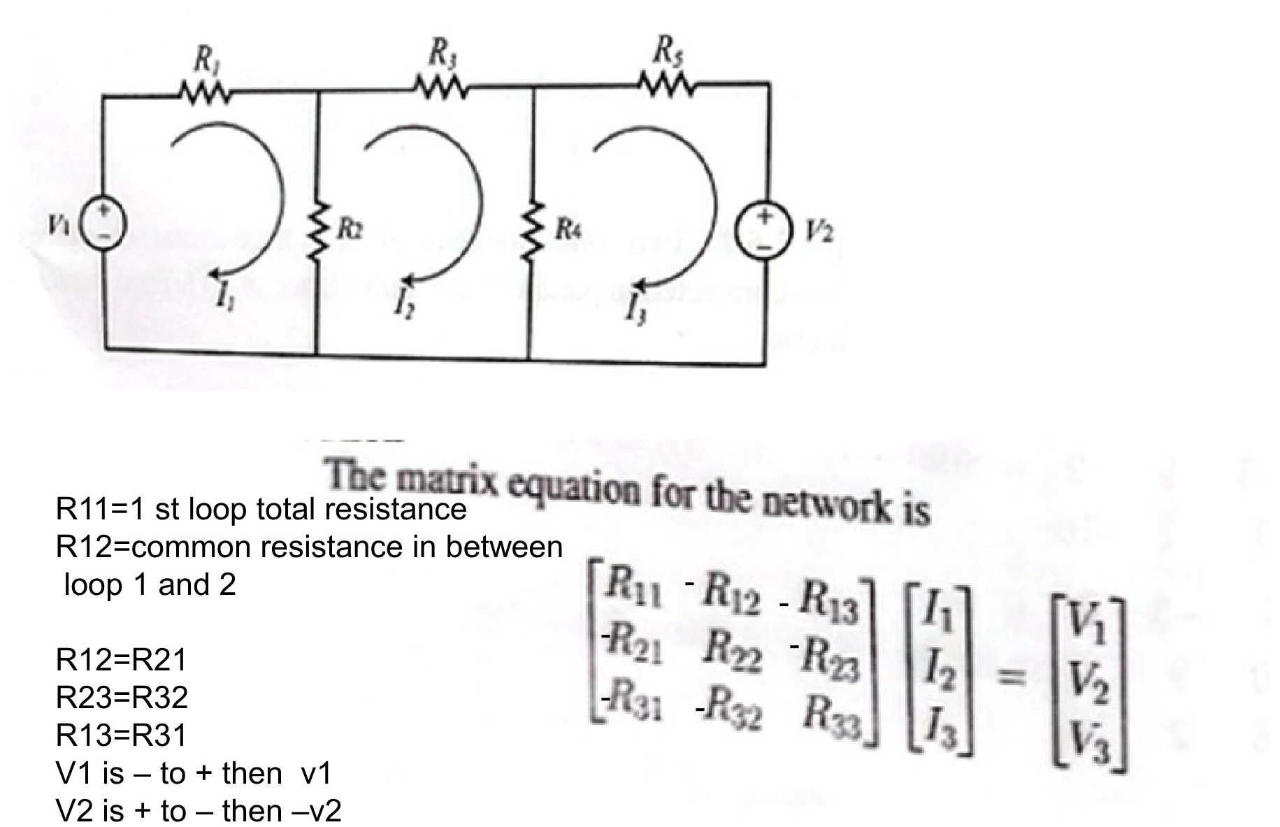
Circuit diagram with three loops containing resistors and voltage sources

The matrix equation for the network is

R11=1st loop total resistanceR_{11} = 1^{\text{st}} \text{ loop total resistance}

R12=common resistance in betweenR_{12} = \text{common resistance in between} loop 1 and 2\text{loop } 1 \text{ and } 2

R12=R21R_{12} = R_{21} R23=R32R_{23} = R_{32} R13=R31R_{13} = R_{31}

V1 is − to + then v1V_1 \text{ is } - \text{ to } + \text{ then } v_1 V2 is + to − then −v2V_2 \text{ is } + \text{ to } - \text{ then } -v_2

[R11−R12−R13−R21R22−R23−R31−R32R33][I1I2I3]=[V1V2V3]\begin{bmatrix} R_{11} & -R_{12} & -R_{13} \\ -R_{21} & R_{22} & -R_{23} \\ -R_{31} & -R_{32} & R_{33} \end{bmatrix} \begin{bmatrix} I_1 \\ I_2 \\ I_3 \end{bmatrix} = \begin{bmatrix} V_1 \\ V_2 \\ V_3 \end{bmatrix}


Page 94 of 185

Matrix form RULE

  • Diagonal Elements (R11,R22,R33R_{11}, R_{22}, R_{33}): Always Positive (++)
    • Sum of all resistances in that specific loop.
  • Off-Diagonal Elements (R12,R23,R31R_{12}, R_{23}, R_{31}, etc.): Usually Negative (−-)
    • Sum of resistances shared between two loops.
    • Sign Rule: If both loop currents pass through the shared resistor in opposite directions, the entry is negative (−-). If they flow in the same direction, the entry is positive (++). Since all mesh currents are drawn clockwise by default, shared branches always have opposing currents, making off-diagonal terms negative.

If two voltage source is same loop For summing voltage element same polarity must be minus the voltage Opposite polarity add the voltage

For voltage matrix voltage polarity is depends on current flow direction


Page 95 of 185

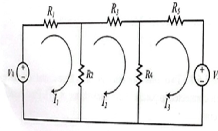
Applying KVL to each mesh, the following equations are obtained.

Circuit diagram with three meshes and mesh currents I1, I2, I3

[R11R12R13R21R22R23R31R32R33][I1I2I3]=[V1V2V3]\begin{bmatrix} R_{11} & R_{12} & R_{13} \\ R_{21} & R_{22} & R_{23} \\ R_{31} & R_{32} & R_{33} \end{bmatrix} \begin{bmatrix} I_1 \\ I_2 \\ I_3 \end{bmatrix} = \begin{bmatrix} V_1 \\ V_2 \\ V_3 \end{bmatrix}

Rearranging the above equations, we can write as

(R_1 + R_2)I_1 &- R_2 I_2 & &= V_1 \\ -R_2 I_1 &+ (R_2 + R_3 + R_4)I_2 &- R_4 I_3 &= 0 \\ &-R_4 I_2 &+ (R_4 + R_5)I_3 &= -V_2 \end{aligned}$ ---

Page 96 of 185

These equations can be represented in matrix form as given below.

[(R1+R2)−R20−R2R2+R3+R4−R40−R4R4+R5][I1I2I3]=[V10−V2]\begin{bmatrix} (R_1 + R_2) & -R_2 & 0 \\ -R_2 & R_2 + R_3 + R_4 & -R_4 \\ 0 & -R_4 & R_4 + R_5 \end{bmatrix} \begin{bmatrix} I_1 \\ I_2 \\ I_3 \end{bmatrix} = \begin{bmatrix} V_1 \\ 0 \\ -V_2 \end{bmatrix}

Page 97 of 185

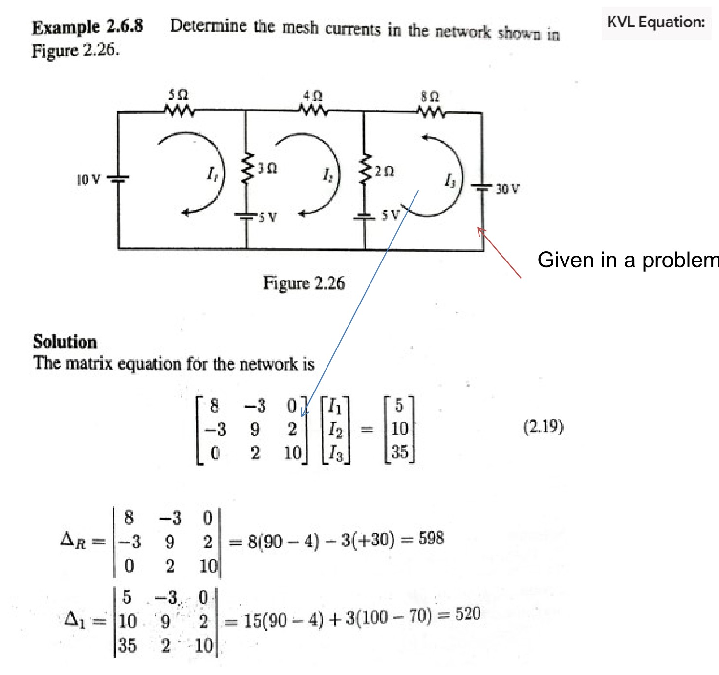
Example 2.6.8 Determine the mesh currents in the network shown in Figure 2.26.
Figure 2.26.

Circuit diagram with three meshes and mesh currents I1, I2, I3

Solution
The matrix equation for the network is
\begin{bmatrix}8&-3&0\\-3&9&2\\0&2&10\end{bmatrix}\begin{bmatrix}I_1\\I_2\\I_3\end{bmatrix}=\begin{bmatrix}5\\10\\35\end{bmatrix}\tag{2.19}

ΔR=∣8−30−3920210∣=8(90−4)−3(+30)=598\Delta_R = \begin{vmatrix} 8 & -3 & 0 \\ -3 & 9 & 2 \\ 0 & 2 & 10 \end{vmatrix} = 8(90 - 4) - 3(+30) = 598

Δ1=∣5−30109235210∣=5(90−4)+3(100−70)=520\Delta_1 = \begin{vmatrix} 5 & -3 & 0 \\ 10 & 9 & 2 \\ 35 & 2 & 10 \end{vmatrix} = 5(90 - 4) + 3(100 - 70) = 520


Page 98 of 185

Δ2=∣850−310203510∣=8(100−70)−5(−30)=390\Delta_2 = \begin{vmatrix} 8 & 5 & 0 \\ -3 & 10 & 2 \\ 0 & 35 & 10 \end{vmatrix} = 8(100 - 70) - 5(-30) = 390

Δ3=∣8−35−39100235∣=8(315−20)+3(−105)+5(−6)=2015\Delta_3 = \begin{vmatrix} 8 & -3 & 5 \\ -3 & 9 & 10 \\ 0 & 2 & 35 \end{vmatrix} = 8(315 - 20) + 3(-105) + 5(-6) = 2015

∴I1=Δ1ΔR=520598=0.87 A\therefore I_1 = \frac{\Delta_1}{\Delta_R} = \frac{520}{598} = 0.87\text{ A}

I2=Δ2ΔR=390598=0.65 AI_2 = \frac{\Delta_2}{\Delta_R} = \frac{390}{598} = 0.65\text{ A}

I3=Δ3ΔR=2015598=3.37 AI_3 = \frac{\Delta_3}{\Delta_R} = \frac{2015}{598} = 3.37\text{ A}


Page 99 of 185

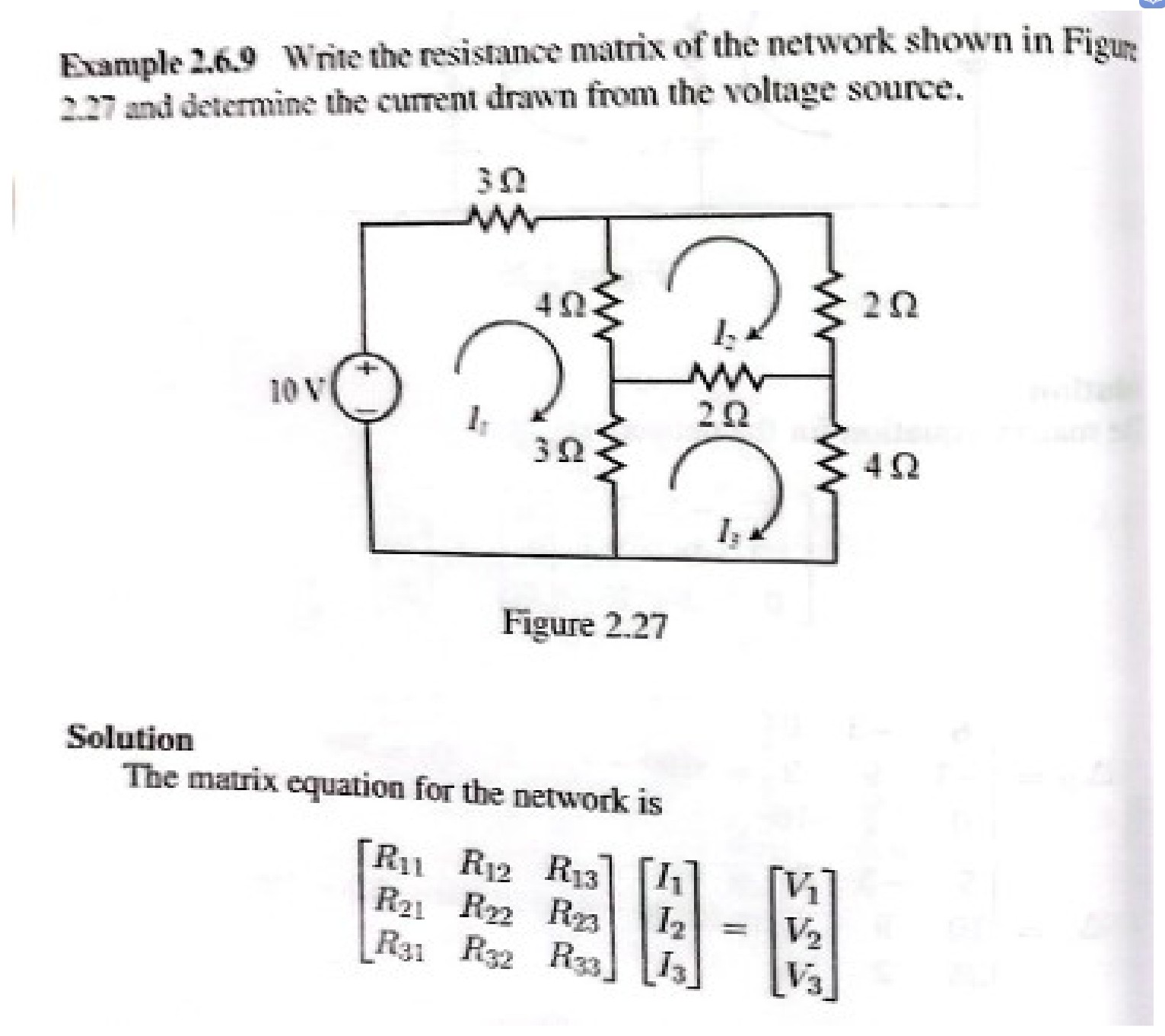
Example 2.6.9 Write the resistance matrix of the network shown in Figure 2.27 and determine the current drawn from the voltage source.

Electrical network diagram with three mesh currents I1, I2, and I3, resistors of 3 ohm, 4 ohm, 2 ohm, 3 ohm, 2 ohm, and 4 ohm, and a 10 V DC voltage source.

Figure 2.27

Solution

The matrix equation for the network is [R11R12R13R21R22R23R31R32R33][I1I2I3]=[V1V2V3]\begin{bmatrix} R_{11} & R_{12} & R_{13} \\ R_{21} & R_{22} & R_{23} \\ R_{31} & R_{32} & R_{33} \end{bmatrix} \begin{bmatrix} I_1 \\ I_2 \\ I_3 \end{bmatrix} = \begin{bmatrix} V_1 \\ V_2 \\ V_3 \end{bmatrix}


Page 100 of 185

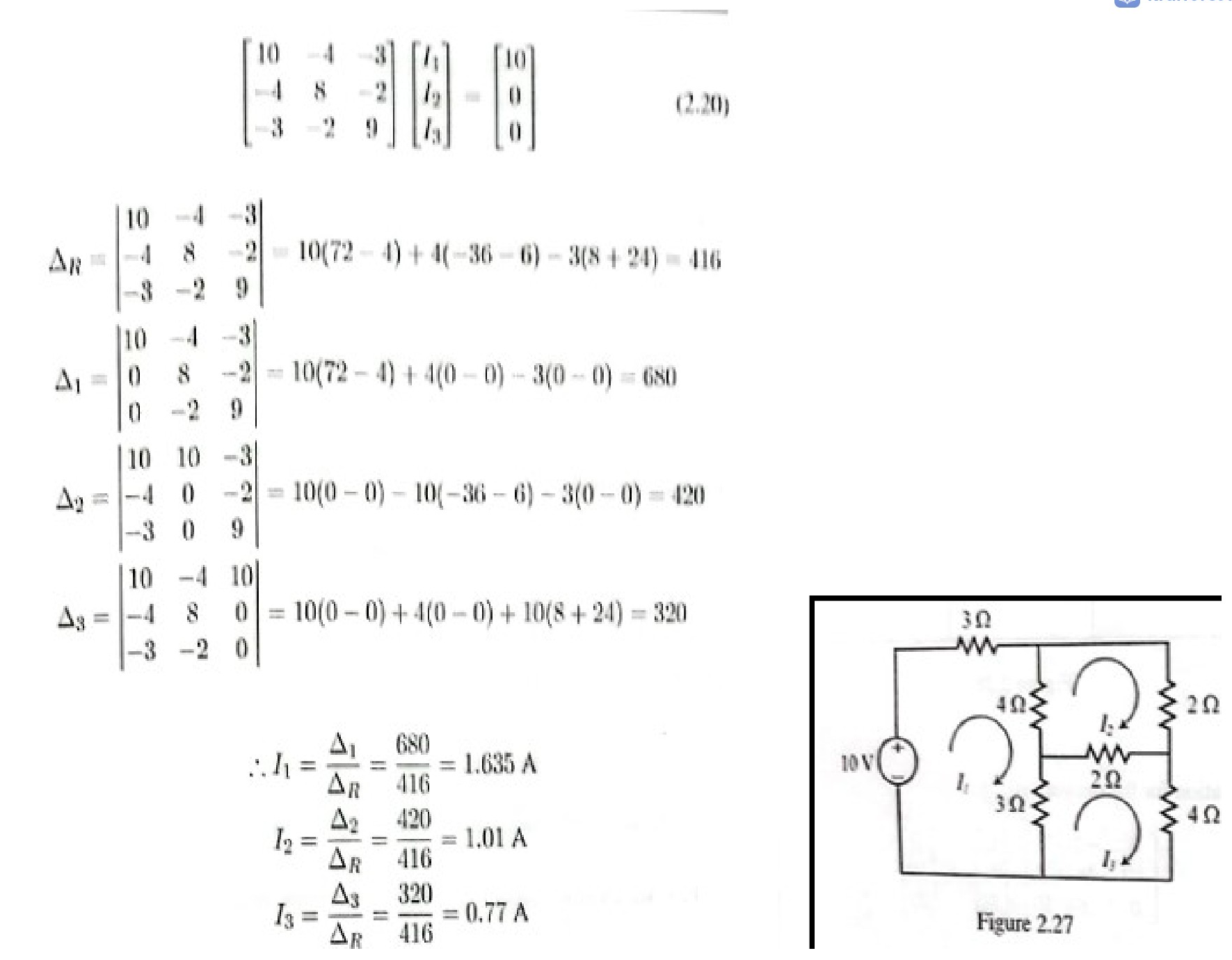
\begin{bmatrix} 10 & -4 & -3 \\ -4 & 8 & -2 \\ -3 & -2 & 9 \end{bmatrix} \begin{bmatrix} I_1 \\ I_2 \\ I_3 \end{bmatrix} = \begin{bmatrix} 10 \\ 0 \\ 0 \end{bmatrix} \tag{2.20}

ΔR=∣10−4−3−48−2−3−29∣=10(72−4)+4(−36−6)−3(8+24)=416\Delta_R = \begin{vmatrix} 10 & -4 & -3 \\ -4 & 8 & -2 \\ -3 & -2 & 9 \end{vmatrix} = 10(72 - 4) + 4(-36 - 6) - 3(8 + 24) = 416

Δ1=∣10−4−308−20−29∣=10(72−4)+4(0−0)−3(0−0)=680\Delta_1 = \begin{vmatrix} 10 & -4 & -3 \\ 0 & 8 & -2 \\ 0 & -2 & 9 \end{vmatrix} = 10(72 - 4) + 4(0 - 0) - 3(0 - 0) = 680

Δ2=∣1010−3−40−2−309∣=10(0−0)−10(−36−6)−3(0−0)=420\Delta_2 = \begin{vmatrix} 10 & 10 & -3 \\ -4 & 0 & -2 \\ -3 & 0 & 9 \end{vmatrix} = 10(0 - 0) - 10(-36 - 6) - 3(0 - 0) = 420

Δ3=∣10−410−480−3−20∣=10(0−0)+4(0−0)+10(8+24)=320\Delta_3 = \begin{vmatrix} 10 & -4 & 10 \\ -4 & 8 & 0 \\ -3 & -2 & 0 \end{vmatrix} = 10(0 - 0) + 4(0 - 0) + 10(8 + 24) = 320

∴I1=Δ1ΔR=680416=1.635 A\therefore I_1 = \frac{\Delta_1}{\Delta_R} = \frac{680}{416} = 1.635\text{ A}

I2=Δ2ΔR=420416=1.01 AI_2 = \frac{\Delta_2}{\Delta_R} = \frac{420}{416} = 1.01\text{ A}

I3=Δ3ΔR=320416=0.77 AI_3 = \frac{\Delta_3}{\Delta_R} = \frac{320}{416} = 0.77\text{ A}

Circuit diagram with mesh currents I1, I2, and I3

Figure 2.27

Page 101 of 185

Home work

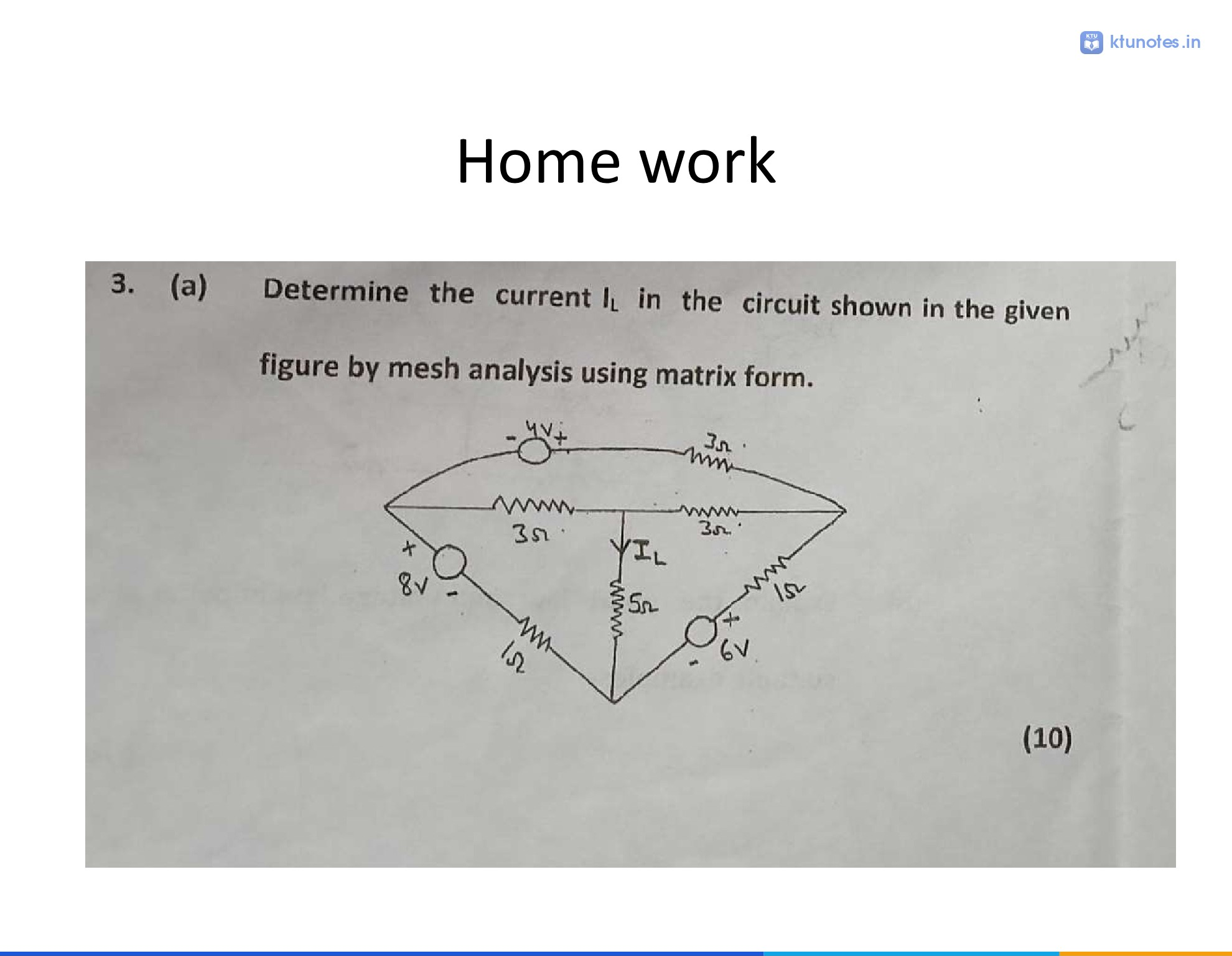
  1. (a) Determine the current ILI_L in the circuit shown in the given figure by mesh analysis using matrix form.

Circuit diagram for mesh analysis with multiple voltage sources and resistors

(10)


Page 102 of 185

KIRCHHOFF'S CURRENT LAW

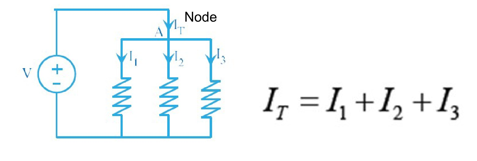
  • Kirchhoff's current law states any current flowing into a node must simultaneously equal the current flowing out of it at any given moment.
  • If entering currents are assigned positive sign, leaving currents will be given negative sign.

Circuit diagram illustrating Kirchhoff's Current Law with a voltage source connected in parallel to three resistor branches, showing a node A with currents I_T entering and I_1, I_2, I_3 leaving.

IT=I1+I2+I3I_T = I_1 + I_2 + I_3


Page 103 of 185

k.c.l Version 2

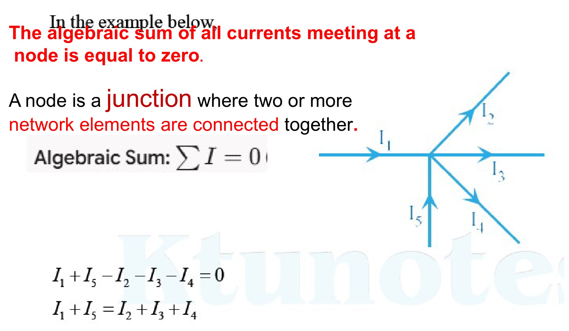
In the example below,

The algebraic sum of all currents meeting at a node is equal to zero.

A node is a junction where two or more network elements are connected together.

Algebraic Sum: ∑I=0\sum I = 0

Current meeting at a node diagram

I1+I5−I2−I3−I4=0I_1 + I_5 - I_2 - I_3 - I_4 = 0 I1+I5=I2+I3+I4I_1 + I_5 = I_2 + I_3 + I_4

Page 104 of 185

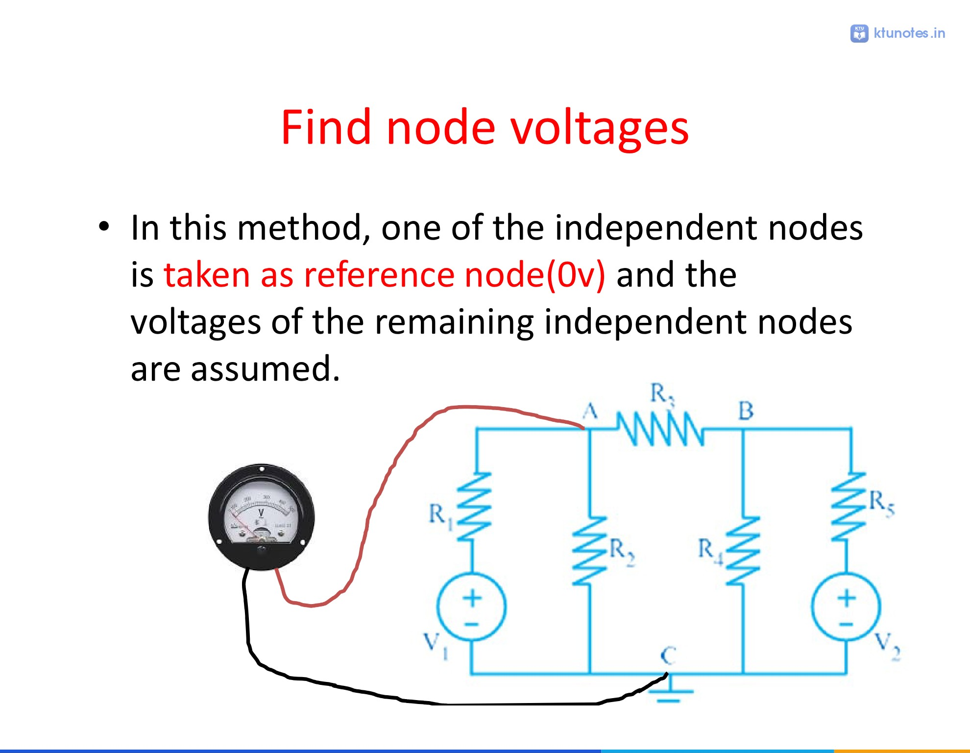
Find node voltages

  • In this method, one of the independent nodes is taken as reference node (0v0\text{v}) and the voltages of the remaining independent nodes are assumed.

Circuit diagram with a voltmeter and nodes A, B, and C


Page 105 of 185

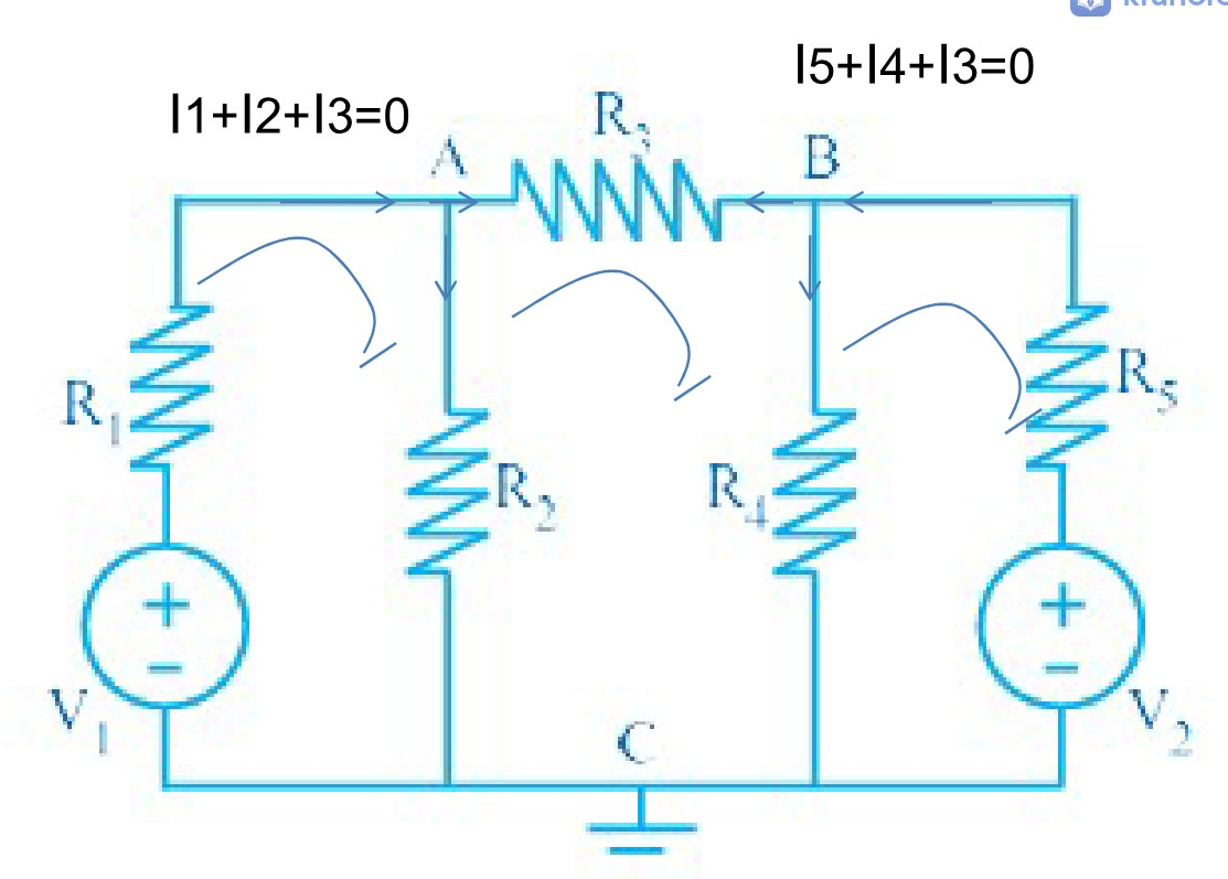
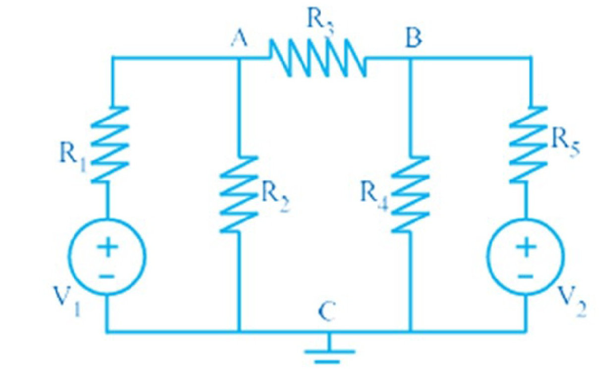
• Consider the following circuit. The circuit has 3 independent nodes A, B and C. Let C be the reference node. Let VA and VB be the potential of A and B with respect to reference node • In node voltage analysis, to identify a node points, current must enter and leave

Circuit diagram with nodes A, B, C, resistors R1 to R5, and voltage sources V1 and V2


Page 106 of 185

Node voltage method step

  • Find the node voltages so we can find the current flow through circuits and components

Circuit diagram for node voltage method analysis showing two voltage sources and five resistors.


Page 107 of 185

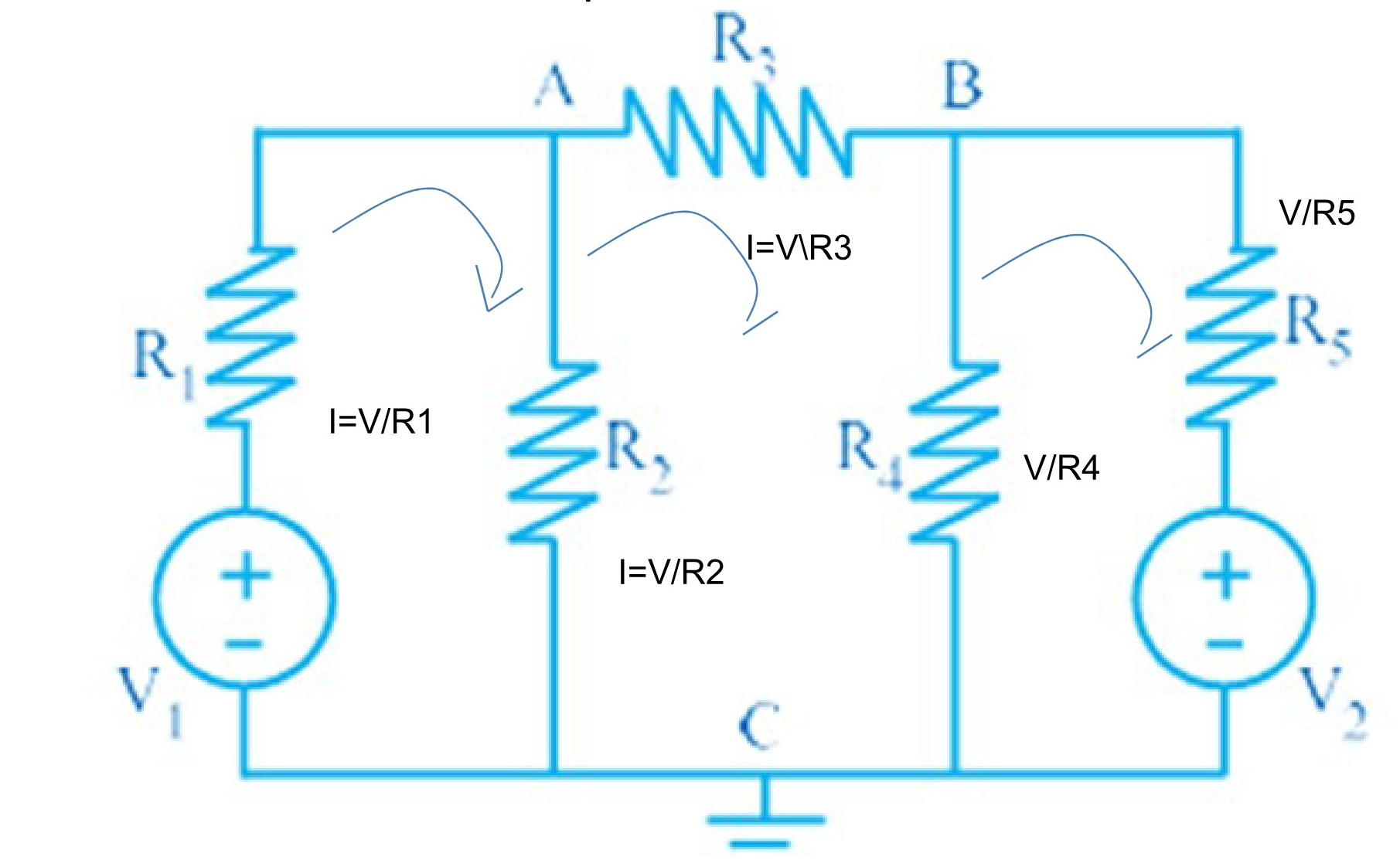
There are two nodes A,B and 1 relative potential and 2 absolute potential differences

Circuit diagram with two voltage sources V1 and V2, five resistors R1 through R5, two nodes A and B, a ground node C, and labeled currents corresponding to each branch.


Page 108 of 185

Three branches connect to node A. Assuming all currents leave node A: A current is I1+I2+I3=0I_1+I_2+I_3=0

  • Left Branch (towards V1V_1): Current flows from potential VAV_A to potential V1V_1 across resistor R1R_1.

Ileft=VA−V1R1I_{\text{left}} = \frac{V_A - V_1}{R_1}

  • Middle-Down Branch (towards Node C): Current flows from VAV_A to ground (0 V0\text{ V}) through R2R_2.

Idown=VA−0R2=VAR2I_{\text{down}} = \frac{V_A - 0}{R_2} = \frac{V_A}{R_2}

  • Right Branch (towards Node B): Current flows from VAV_A to VBV_B across R3R_3.

Iright=VA−VBR3I_{\text{right}} = \frac{V_A - V_B}{R_3}


Page 109 of 185

Circuit diagram with two nodes A and B, resistors R1 to R5, voltage sources V1 and V2, and a ground reference C.

Applying KCL at node A, →I1+I2+I3=0→I=V/R\rightarrow I_1 + I_2 + I_3 = 0 \rightarrow I = V/R

VA−V1R1+VAR2+VA−VBR3=0\frac{V_A - V_1}{R_1} + \frac{V_A}{R_2} + \frac{V_A - V_B}{R_3} = 0

Applying KCL at node B,

VB−V2R5+VBR4+VB−VAR3=0\frac{V_B - V_2}{R_5} + \frac{V_B}{R_4} + \frac{V_B - V_A}{R_3} = 0

By solving the two equations, we can determine VAV_A and VBV_B.


Page 110 of 185

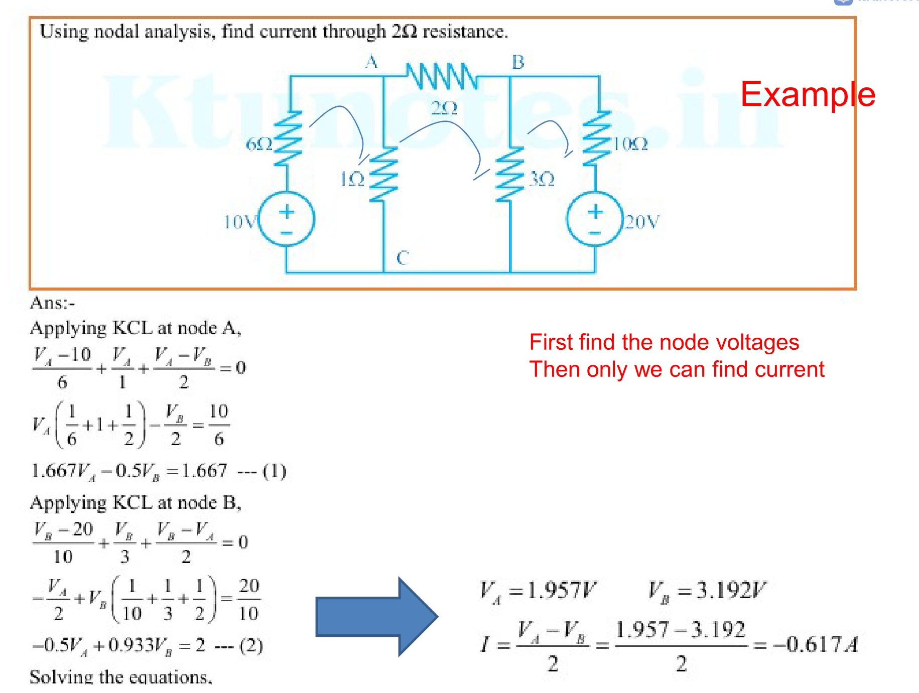
Using nodal analysis, find current through 2Ω2\Omega resistance.

Circuit diagram with nodes A, B, and C, resistors of 6 ohms, 1 ohm, 2 ohms, 3 ohms, and 10 ohms, and DC voltage sources of 10V and 20V.

Example

First find the node voltages Then only we can find current

Ans:-

Applying KCL at node A, VA−106+VA1+VA−VB2=0\frac{V_A - 10}{6} + \frac{V_A}{1} + \frac{V_A - V_B}{2} = 0

VA(16+1+12)−VB2=106V_A \left( \frac{1}{6} + 1 + \frac{1}{2} \right) - \frac{V_B}{2} = \frac{10}{6}

1.667VA−0.5VB=1.667−−−(1)1.667 V_A - 0.5 V_B = 1.667 \quad ---\text{(1)}

Applying KCL at node B, VB−2010+VB3+VB−VA2=0\frac{V_B - 20}{10} + \frac{V_B}{3} + \frac{V_B - V_A}{2} = 0

−VA2+VB(110+13+12)=2010-\frac{V_A}{2} + V_B \left( \frac{1}{10} + \frac{1}{3} + \frac{1}{2} \right) = \frac{20}{10}

−0.5VA+0.933VB=2−−−(2)-0.5 V_A + 0.933 V_B = 2 \quad ---\text{(2)}

Solving the equations,

VA=1.957V,VB=3.192VV_A = 1.957\text{V}, \quad V_B = 3.192\text{V}

I=VA−VB2=1.957−3.1922=−0.617AI = \frac{V_A - V_B}{2} = \frac{1.957 - 3.192}{2} = -0.617\text{A}


Page 111 of 185

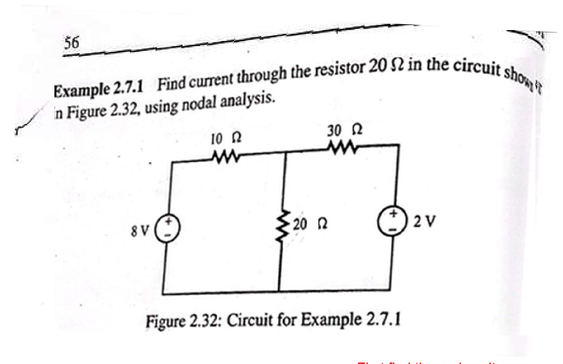
Example 2.7.1 Find current through the resistor 20   \Omega20\ \text{ }\ \text{\Omega} in the circuit shown in Figure 2.32, using nodal analysis.

Circuit diagram with resistors and voltage sources

Figure 2.32: Circuit for Example 2.7.1

First find the node voltages Then only we can find current


Page 112 of 185

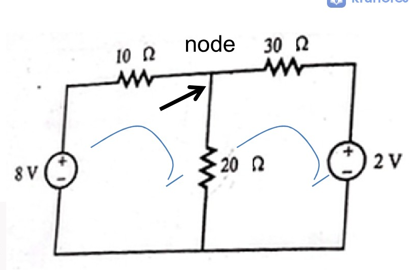
e node V1V_1:

V1−810+V120+V1−230=0\frac{V_1 - 8}{10} + \frac{V_1}{20} + \frac{V_1 - 2}{30} = 0

Electrical circuit diagram showing an 8V source, 10 ohm resistor, 20 ohm resistor, 30 ohm resistor, and a 2V source connected in a loop with a central node labeled node V1.

Step 2: Solve for Node Voltage V1V_1

Multiply the entire equation by the common denominator 6060 to clear fractions:

6(V1−8)+3V1+2(V1−2)=06(V_1 - 8) + 3V_1 + 2(V_1 - 2) = 0

6V1−48+3V1+2V1−4=06V_1 - 48 + 3V_1 + 2V_1 - 4 = 0

11V1−52=011V_1 - 52 = 0

11V1=5211V_1 = 52

Step 3: Calculate Current through the 20 Ω20\ \text{}\Omega Resistor

The current flowing downward through the 20 Ω20\ \text{}\Omega resistor is:

I20 Ω=V120=4.72720≈0.236 A(or 1355 A)I_{20\ \text{}\Omega} = \frac{V_1}{20} = \frac{4.727}{20} \approx 0.236\ \text{A} \quad \left(\text{or}\ \frac{13}{55}\ \text{A}\right)

The current through the 20 Ω20\ \text{}\Omega resistor is 0.236 A0.236\ \text{A} (flowing downwards).


Page 113 of 185

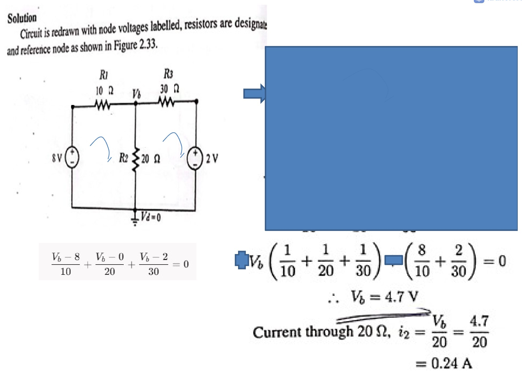
Solution

Circuit is redrawn with node voltages labelled, resistors are designated and reference node as shown in Figure 2.33.

Electrical circuit diagram with a node voltage V_b and reference node V_d = 0

Vb−810+Vb−020+Vb−230=0\frac{V_b - 8}{10} + \frac{V_b - 0}{20} + \frac{V_b - 2}{30} = 0

Vb(110+120+130)−(810+230)=0V_b \left(\frac{1}{10} + \frac{1}{20} + \frac{1}{30}\right) - \left(\frac{8}{10} + \frac{2}{30}\right) = 0

∴Vb=4.7 V\therefore V_b = 4.7\text{ V}

Current through 20 Ω, i2=Vb20=4.720=0.24 A\text{Current through } 20\text{ }\Omega,\ i_2 = \frac{V_b}{20} = \frac{4.7}{20} = 0.24\text{ A}


Page 114 of 185

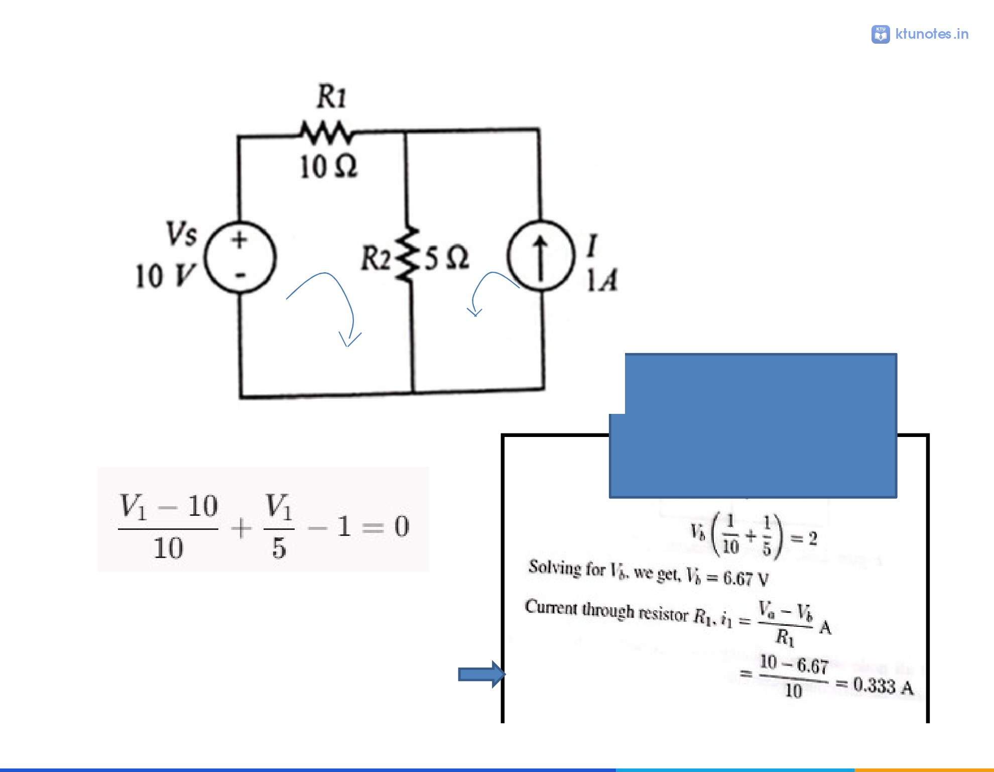
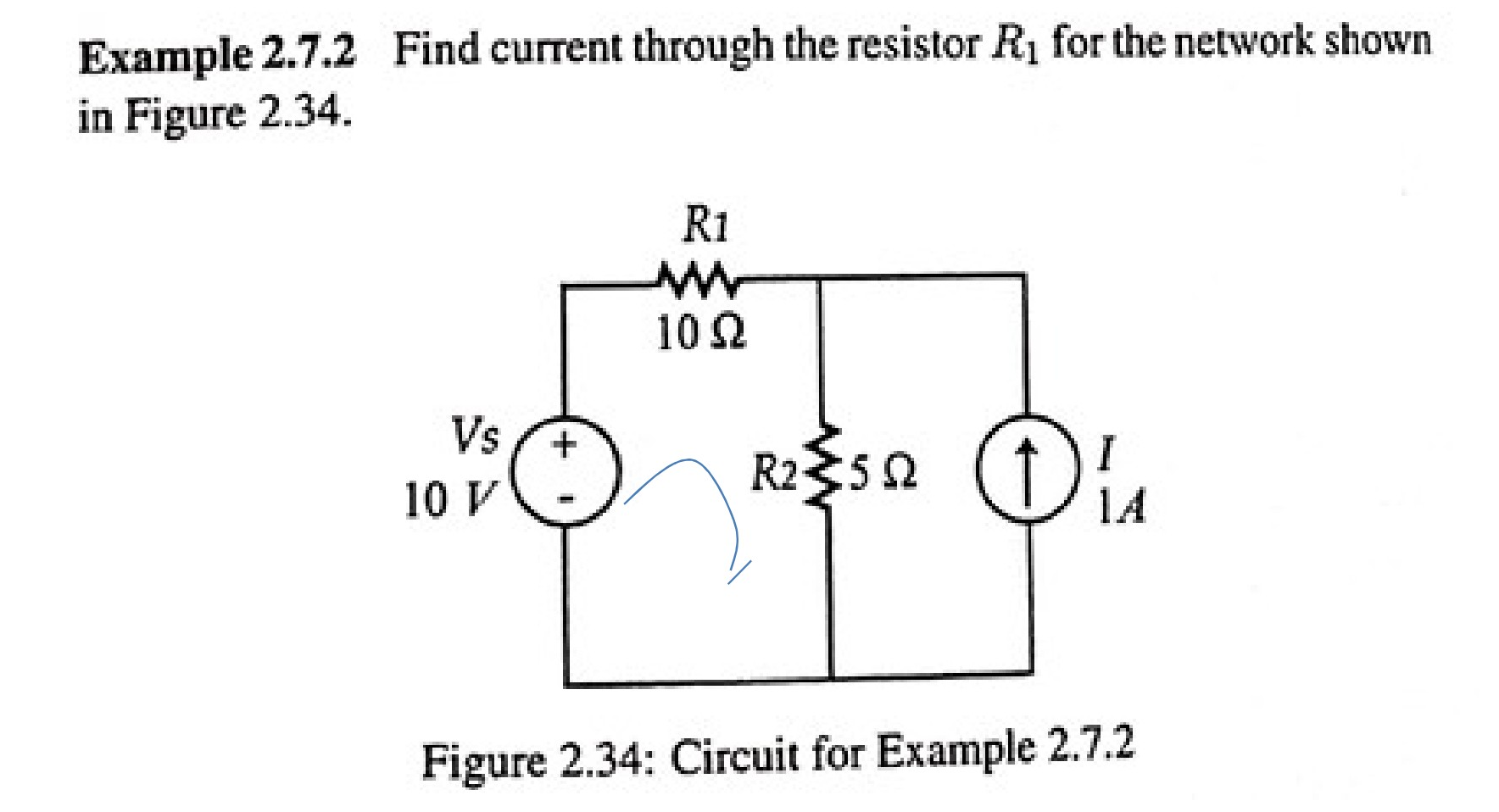
Example 2.7.2 Find current through the resistor R1R_1 for the network shown in Figure 2.34.

Circuit diagram with a voltage source, a current source, and two resistors

Figure 2.34: Circuit for Example 2.7.2

First find the node voltages Then only we can find current


Page 115 of 185

Circuit diagram with a voltage source, two resistors, and a current source

V1−1010+V15−1=0\frac{V_1 - 10}{10} + \frac{V_1}{5} - 1 = 0

Vb(110+15)=2V_b \left(\frac{1}{10} + \frac{1}{5}\right) = 2

Solving for VbV_b, we get, Vb=6.67 VV_b = 6.67\text{ V}

Current through resistor R1R_1, i1=Va−VbR1 Ai_1 = \frac{V_a - V_b}{R_1}\text{ A}

=10−6.6710=0.333 A= \frac{10 - 6.67}{10} = 0.333\text{ A}


Page 116 of 185

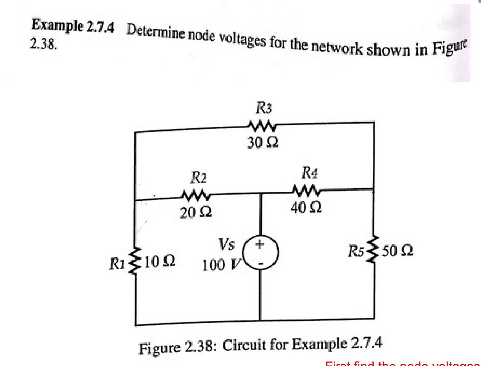
Example 2.7.4 Determine node voltages for the network shown in Figure 2.38.

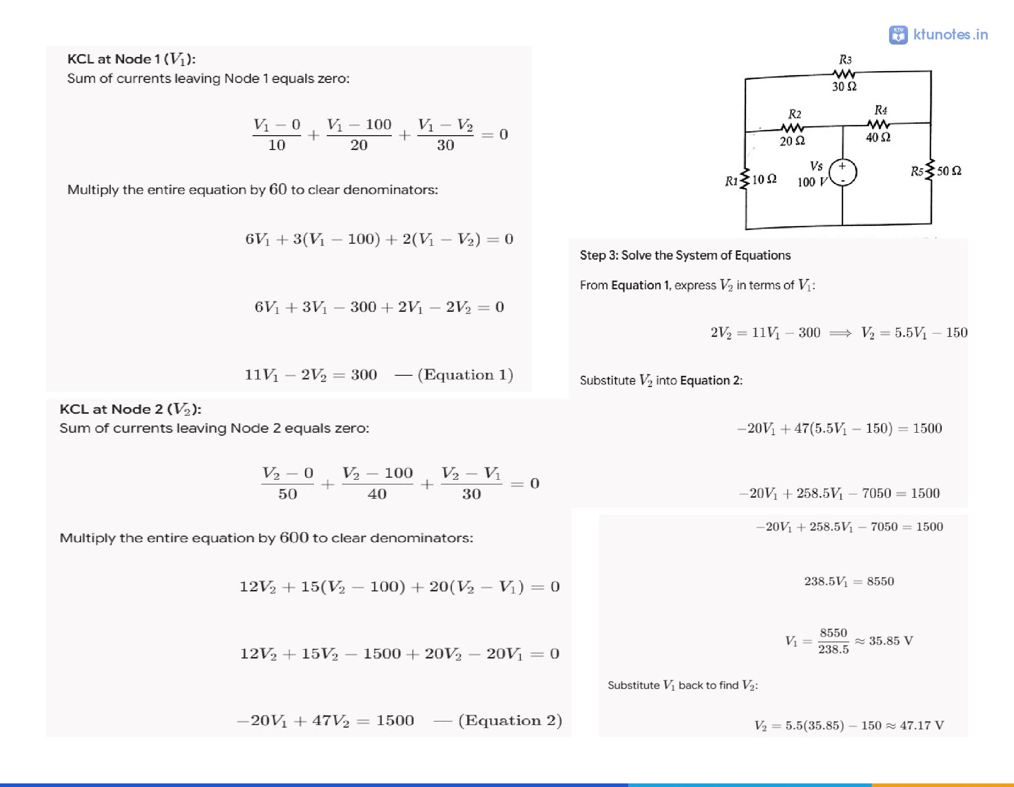
Circuit diagram with resistors R1=10 ohms, R2=20 ohms, R3=30 ohms, R4=40 ohms, R5=50 ohms, and a DC voltage source Vs=100V.

Figure 2.38: Circuit for Example 2.7.4

First find the node voltages Then only we can find current


Page 117 of 185

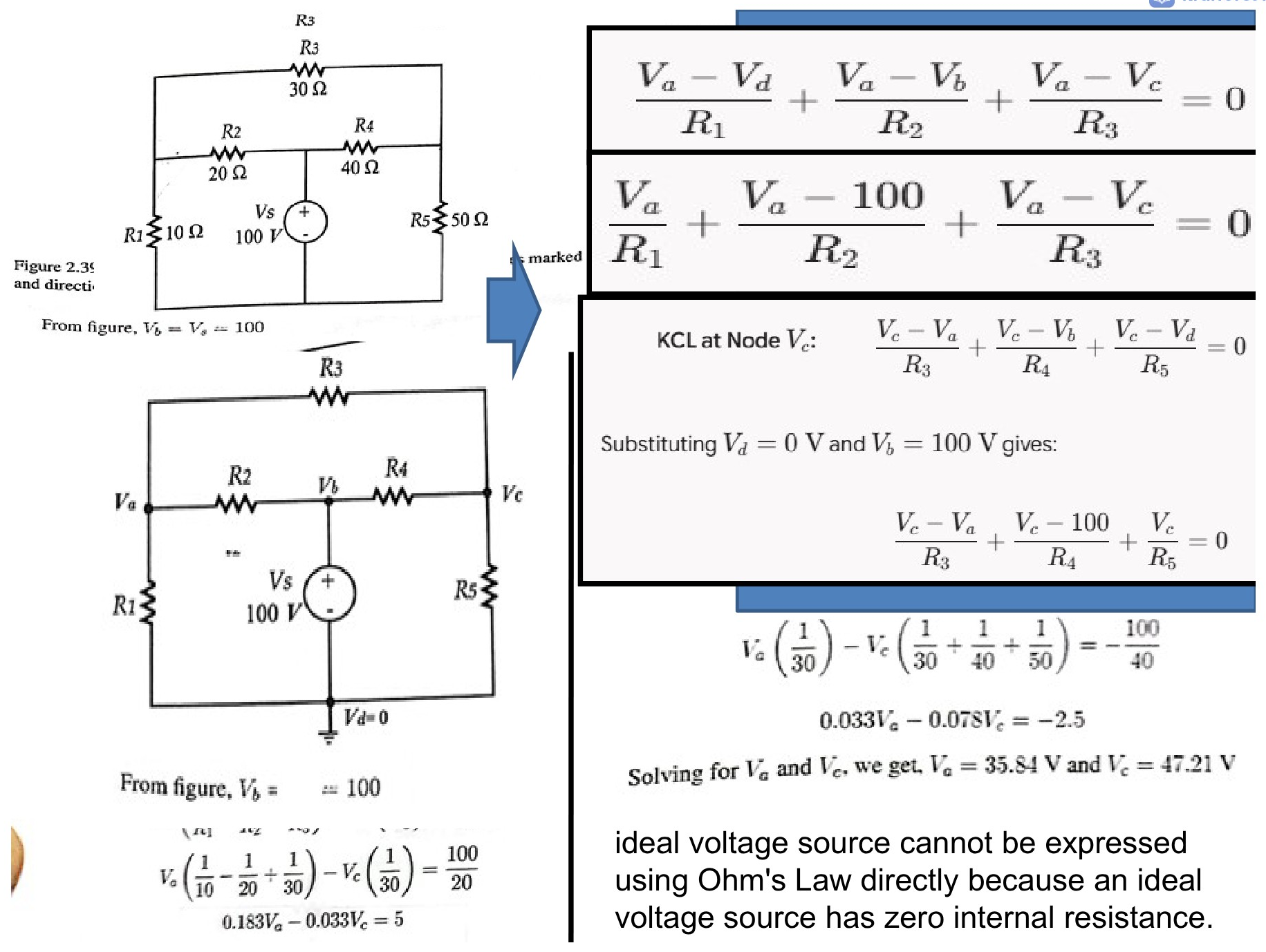
Figure 2.39 and directi

From figure, Vb=Vs=100V_b = V_s = 100

Circuit diagram with nodes labeled V_a, V_b, V_c, V_d=0, resistors R1 through R5, and a voltage source V_s of 100 V.

From figure, Vb=100V_b = 100

Va(110−120+130)−Vc(130)=10020V_a \left(\frac{1}{10} - \frac{1}{20} + \frac{1}{30}\right) - V_c \left(\frac{1}{30}\right) = \frac{100}{20} 0.183Va−0.033Vc=50.183V_a - 0.033V_c = 5

Va−VdR1+Va−VbR2+Va−VcR3=0\frac{V_a - V_d}{R_1} + \frac{V_a - V_b}{R_2} + \frac{V_a - V_c}{R_3} = 0

VaR1+Va−100R2+Va−VcR3=0\frac{V_a}{R_1} + \frac{V_a - 100}{R_2} + \frac{V_a - V_c}{R_3} = 0

KCL at Node VcV_c: Vc−VaR3+Vc−VbR4+Vc−VdR5=0\frac{V_c - V_a}{R_3} + \frac{V_c - V_b}{R_4} + \frac{V_c - V_d}{R_5} = 0

Substituting Vd=0 VV_d = 0\text{ V} and Vb=100 VV_b = 100\text{ V} gives:

Vc−VaR3+Vc−100R4+VcR5=0\frac{V_c - V_a}{R_3} + \frac{V_c - 100}{R_4} + \frac{V_c}{R_5} = 0

Va(130)−Vc(130+140+150)=−10040V_a \left(\frac{1}{30}\right) - V_c \left(\frac{1}{30} + \frac{1}{40} + \frac{1}{50}\right) = - \frac{100}{40}

0.033Va−0.078Vc=−2.50.033V_a - 0.078V_c = -2.5

Solving for VaV_a and VcV_c, we get, Va=35.84 VV_a = 35.84\text{ V} and Vc=47.21 VV_c = 47.21\text{ V}

ideal voltage source cannot be expressed using Ohm's Law directly because an ideal voltage source has zero internal resistance.


Page 118 of 185

KCL at Node 1 (V1V_1): Sum of currents leaving Node 1 equals zero: V1−010+V1−10020+V1−V230=0\frac{V_1 - 0}{10} + \frac{V_1 - 100}{20} + \frac{V_1 - V_2}{30} = 0

Multiply the entire equation by 6060 to clear denominators: 6V1+3(V1−100)+2(V1−V2)=06V_1 + 3(V_1 - 100) + 2(V_1 - V_2) = 0 6V1+3V1−300+2V1−2V2=06V_1 + 3V_1 - 300 + 2V_1 - 2V_2 = 0 11V1−2V2=300−(Equation 1)11V_1 - 2V_2 = 300 \quad - (\text{Equation } 1)

KCL at Node 2 (V2V_2): Sum of currents leaving Node 2 equals zero: V2−050+V2−10040+V2−V130=0\frac{V_2 - 0}{50} + \frac{V_2 - 100}{40} + \frac{V_2 - V_1}{30} = 0

Multiply the entire equation by 600600 to clear denominators: 12V2+15(V2−100)+20(V2−V1)=012V_2 + 15(V_2 - 100) + 20(V_2 - V_1) = 0 12V2+15V2−1500+20V2−20V1=012V_2 + 15V_2 - 1500 + 20V_2 - 20V_1 = 0 −20V1+47V2=1500−(Equation 2)-20V_1 + 47V_2 = 1500 \quad - (\text{Equation } 2)

Circuit diagram with resistors and a DC voltage source

Step 3: Solve the System of Equations From Equation 1, express V2V_2 in terms of V1V_1: 2V2=11V1−300  ⟹  V2=5.5V1−1502V_2 = 11V_1 - 300 \implies V_2 = 5.5V_1 - 150

Substitute V2V_2 into Equation 2: −20V1+47(5.5V1−150)=1500-20V_1 + 47(5.5V_1 - 150) = 1500 −20V1+258.5V1−7050=1500-20V_1 + 258.5V_1 - 7050 = 1500 −20V1+258.5V1−7050=1500-20V_1 + 258.5V_1 - 7050 = 1500 238.5V1=8550238.5V_1 = 8550 V1=8550238.5≈35.85 VV_1 = \frac{8550}{238.5} \approx 35.85 \text{ V}

Substitute V1V_1 back to find V2V_2: V2=5.5(35.85)−150≈47.17 VV_2 = 5.5(35.85) - 150 \approx 47.17 \text{ V}


Page 119 of 185

Nodal voltage Matrix representation

In general, for any circuit, the node voltage equation can be written as V/R=IV/R=I G×V=ISG \times V = I_S

where

G=[G11−G12…−G1n−G21G22…−Gnn…………Gn1−Gn2…Gnn]G = \begin{bmatrix} G_{11} & -G_{12} & \dots & -G_{1n} \\ -G_{21} & G_{22} & \dots & -G_{nn} \\ \dots & \dots & \dots & \dots \\ G_{n1} & -G_{n2} & \dots & G_{nn} \end{bmatrix}

Matrix GG is called the conductance matrix.

conductance, G=1RG = \frac{1}{R},

V=[V1V2…Vn]V = \begin{bmatrix} V_1 \\ V_2 \\ \dots \\ V_n \end{bmatrix}

IS=[IS1IS2…ISn]I_S = \begin{bmatrix} I_{S1} \\ I_{S2} \\ \dots \\ I_{Sn} \end{bmatrix}


Page 120 of 185

Compare mesh current matrix node voltage matrix

FeatureMesh Current Matrix Method [R][I]=[V][R][I] = [V]Node Voltage Matrix Method [G][V]=[I][G][V] = [I]
Governing LawKirchhoff's Voltage Law (KVL) around loopsKirchhoff's Current Law (KCL) at nodes
Unknown Vector (X)(X)Mesh currents [I1,I2,...,Im]T[I_1, I_2, \bm{\text{...}}, I_m]^TNon-reference node voltages [V1,V2,...,Vn]T[V_1, V_2, \bm{\text{...}}, V_n]^T
Coefficient Matrix (A)(A)Resistance Matrix [R][R] (Units: Ohms, Ω\Omega)Conductance Matrix [G][G] (Units: Siemens, SS)
Diagonal Elements (Aii)(A_{ii})Sum of resistances in Mesh ii (Always positive)Sum of conductances connected to Node ii (Always positive)
Off-Diagonal Elements (AijA_{ij})Negative sum of resistances shared between Mesh ii and Mesh jjNegative sum of conductances connected directly between Node ii and Node jj
Source Vector (B)(B)Net driving voltage in each mesh [V][V]Net injected current into each node [I][I]

Page 121 of 185

Matrix Formats

  1. Mesh Current Matrix Equation
R_{11} & R_{12} & \\tau & R_{1m} \ R_{21} & R_{22} & \\tau & R_{2m} \\\vdots & \vdots & \ddots & \vdots \ R_{m1} & R_{m2} & \\tau & R_{mm} \end{bmatrix} \begin{bmatrix} I_1 \ I_2 \ \vdots \ I_m \end{bmatrix} = \begin{bmatrix} V_{s1} \ V_{s2} \ \vdots \ V_{sm} \end{bmatrix}$ * $R_{ii}$: Sum of all branch resistances bounding mesh $i$. * $R_{ij}$ ($i \neq j$): $-(\text{resistance shared by mesh } i \text{ and mesh } j)$ when both mesh currents are defined clockwise. * $V_{si}$: Sum of independent voltage source rises in the direction of mesh current $i$. 2. Node Voltage Matrix Equation $\begin{bmatrix} G_{11} & G_{12} & \dots & G_{1n} \ G_{21} & G_{22} & \dots & G_{2n} \ \vdots & \vdots & \ddots & \vdots \ G_{n1} & G_{n2} & \dots & G_{nn} \end{bmatrix} \begin{bmatrix} V_1 \ V_2 \ \vdots \ V_n \end{bmatrix} = \begin{bmatrix} I_{s1} \ I_{s2} \ \vdots \ I_{sn} \end{bmatrix}$ * $G_{ii}$: Sum of conductances ($1/R$) connected to node $i$. * $G_{ij}$ ($i \neq j$): $-(\text{conductance connected directly between node } i \text{ and node } j)$. * $I_{si}$: Net sum of independent source currents entering node $i$. ---

Page 122 of 185

Comparing Mesh Analysis and Nodal Analysis

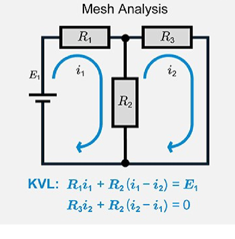
Mesh Analysis

Mesh analysis circuit diagram showing two loops with currents i1 and i2, resistors R1, R2, R3, and a voltage source E1

KVL: R1i1+R2(i1−i2)=E1\text{KVL: } R_1 i_1 + R_2(i_1 - i_2) = E_1

R3i2+R2(i2−i1)=0R_3 i_2 + R_2(i_2 - i_1) = 0

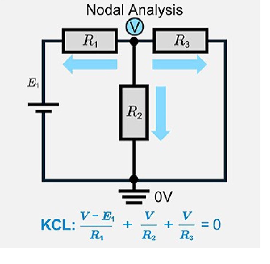
Nodal Analysis

Nodal analysis circuit diagram showing node voltage V, reference ground at 0V, resistors R1, R2, R3, voltage source E1, and branch current direction arrows

KCL: V−E1R1+VR2+VR3=0\text{KCL: } \frac{V - E_1}{R_1} + \frac{V}{R_2} + \frac{V}{R_3} = 0


Page 123 of 185

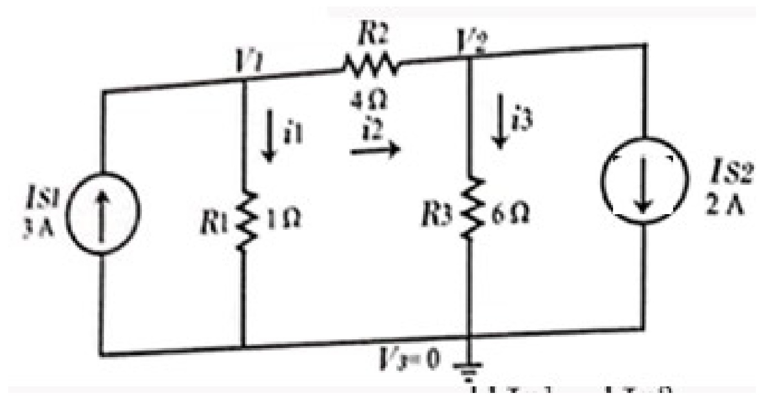
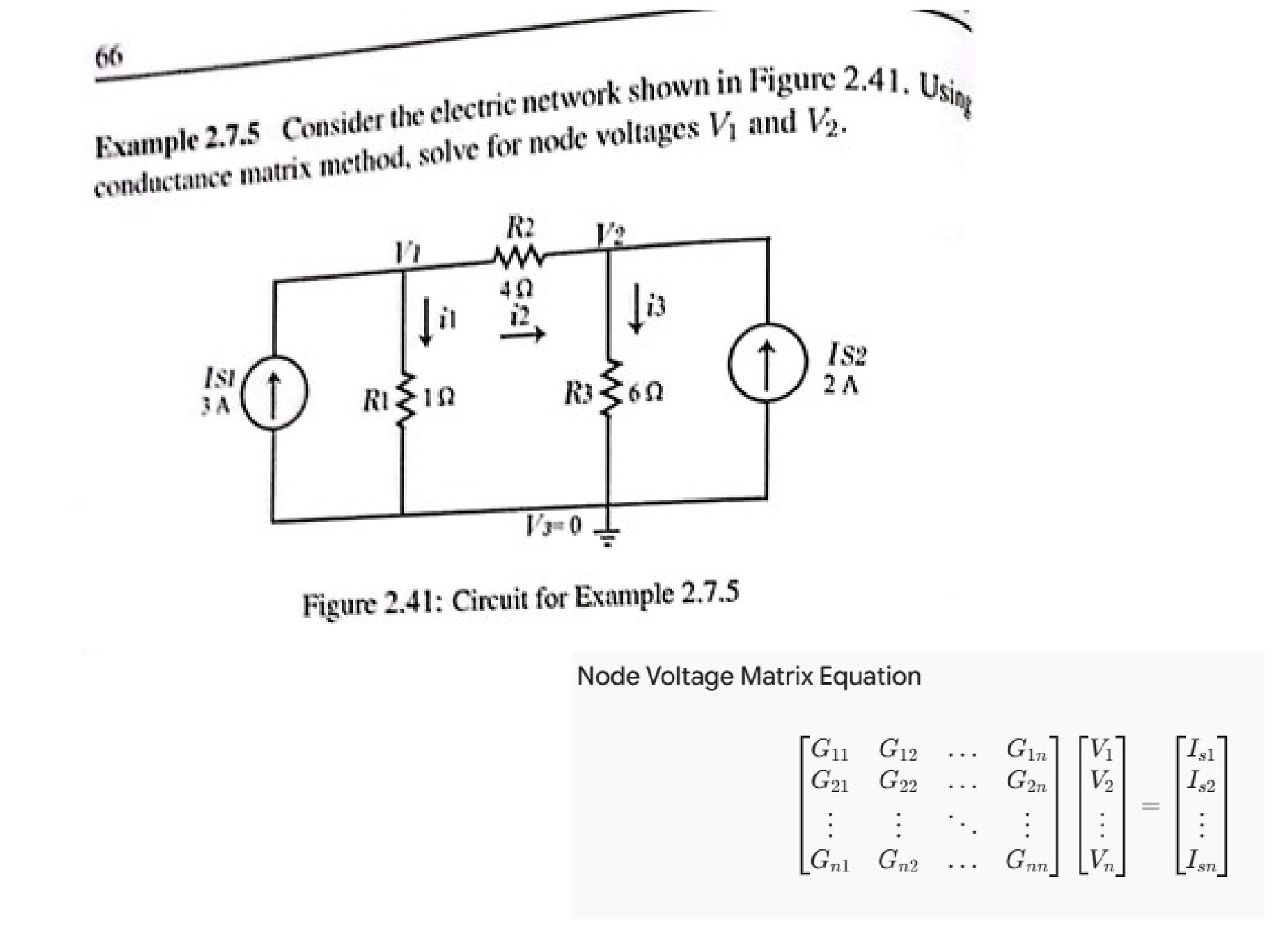
Example 2.7.5 Consider the electric network shown in Figure 2.41. Using conductance matrix method, solve for node voltages V1V_1 and V2V_2.

Circuit diagram for Example 2.7.5 showing a network with two current sources, three resistors, and labeled node voltages V1, V2, and V3=0.

Figure 2.41: Circuit for Example 2.7.5

Node Voltage Matrix Equation

[G11G12…G1nG21G22…G2n⋮⋮⋱⋮Gn1Gn2…Gnn][V1V2⋮Vn]=[Is1Is2⋮Isn]\begin{bmatrix} G_{11} & G_{12} & \dots & G_{1n} \\ G_{21} & G_{22} & \dots & G_{2n} \\ \vdots & \vdots & \ddots & \vdots \\ G_{n1} & G_{n2} & \dots & G_{nn} \end{bmatrix} \begin{bmatrix} V_1 \\ V_2 \\ \vdots \\ V_n \end{bmatrix} = \begin{bmatrix} I_{s1} \\ I_{s2} \\ \vdots \\ I_{sn} \end{bmatrix}


Page 124 of 185

Solution

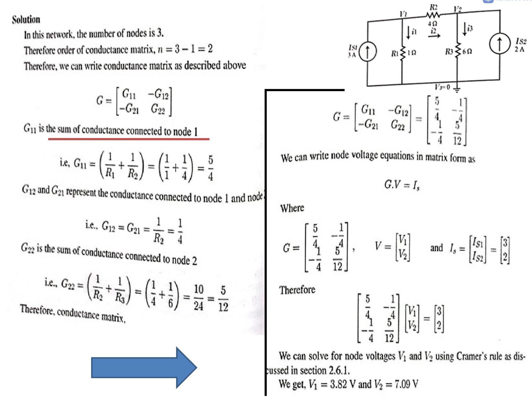
In this network, the number of nodes is 33.

Therefore order of conductance matrix, n=3−1=2n = 3 - 1 = 2

Therefore, we can write conductance matrix as described above

G=[G11−G12−G21G22]G = \begin{bmatrix} G_{11} & -G_{12} \\ -G_{21} & G_{22} \end{bmatrix}

G11G_{11} is the sum of conductance connected to node 1

i.e., G11=(1R1+1R2)=(1+14)=54G_{11} = \left(\frac{1}{R_1} + \frac{1}{R_2}\right) = \left(1 + \frac{1}{4}\right) = \frac{5}{4}

G12G_{12} and G21G_{21} represent the conductance connected to node 1 and node 2

i.e., G12=G21=1R2=14G_{12} = G_{21} = \frac{1}{R_2} = \frac{1}{4}

G22G_{22} is the sum of conductance connected to node 2

i.e., G22=(1R2+1R3)=(14+16)=1024=512G_{22} = \left(\frac{1}{R_2} + \frac{1}{R_3}\right) = \left(\frac{1}{4} + \frac{1}{6}\right) = \frac{10}{24} = \frac{5}{12}

Therefore, conductance matrix,

Electrical circuit diagram with current sources and resistors

G=[G11−G12−G21G22]=[54−14−14512]G = \begin{bmatrix} G_{11} & -G_{12} \\ -G_{21} & G_{22} \end{bmatrix} = \begin{bmatrix} \frac{5}{4} & -\frac{1}{4} \\ -\frac{1}{4} & \frac{5}{12} \end{bmatrix}

We can write node voltage equations in matrix form as

G.V=IsG.V = I_s

Where

G=[54−14−14512],V=[V1V2],and Is=[IS1IS2]=[32]G = \begin{bmatrix} \frac{5}{4} & -\frac{1}{4} \\ -\frac{1}{4} & \frac{5}{12} \end{bmatrix}, \quad V = \begin{bmatrix} V_1 \\ V_2 \end{bmatrix}, \quad \text{and } I_s = \begin{bmatrix} I_{S1} \\ I_{S2} \end{bmatrix} = \begin{bmatrix} 3 \\ 2 \end{bmatrix}

Therefore

[54−14−14512][V1V2]=[32]\begin{bmatrix} \frac{5}{4} & -\frac{1}{4} \\ -\frac{1}{4} & \frac{5}{12} \end{bmatrix} \begin{bmatrix} V_1 \\ V_2 \end{bmatrix} = \begin{bmatrix} 3 \\ 2 \end{bmatrix}

We can solve for node voltages V1V_1 and V2V_2 using Cramer's rule as discussed in section 2.6.1.

We get, V1=3.82 VV_1 = 3.82\text{ V} and V2=7.09 VV_2 = 7.09\text{ V}


Page 125 of 185

Next problem

Electrical circuit diagram with current sources, resistors, and node voltages


Page 126 of 185

  1. Conductance Terms (GijG_{ij}):
  • G11=Sum of conductances connected to Node 1=1R1+1R2=14+14=1.25 SG_{11} = \text{Sum of conductances connected to Node } 1 = \frac{1}{R_1} + \frac{1}{R_2} = \frac{1}{4} + \frac{1}{4} = 1.25\text{ S}
  • G22=Sum of conductances connected to Node 2=1R2+1R3=14+16=512 S≈0.4167 SG_{22} = \text{Sum of conductances connected to Node } 2 = \frac{1}{R_2} + \frac{1}{R_3} = \frac{1}{4} + \frac{1}{6} = \frac{5}{12}\text{ S} \approx 0.4167\text{ S}
  • G12=G21=−Conductance between Node 1 and Node 2=−1R2=−14=−0.25 SG_{12} = G_{21} = -\text{Conductance between Node } 1 \text{ and Node } 2 = -\frac{1}{R_2} = -\frac{1}{4} = -0.25\text{ S}
  1. Source Currents (IsiI_{si}):
  • Is1=Net current entering Node 1=3 A (from IS1)I_{s1} = \text{Net current entering Node } 1 = 3\text{ A } (\text{from } I_{S1})
  • Is2=Net current entering Node 2=−2 A (since IS2=2 A leaves Node 2)I_{s2} = \text{Net current entering Node } 2 = -2\text{ A } (\text{since } I_{S2} = 2\text{ A leaves Node } 2)

the matrix equation:

[1.25−0.25−0.25512][V1V2]=[3−2]\begin{bmatrix} 1.25 & -0.25 \\ -0.25 & \frac{5}{12} \end{bmatrix} \begin{bmatrix} V_1 \\ V_2 \end{bmatrix} = \begin{bmatrix} 3 \\ -2 \end{bmatrix}


Page 127 of 185

Using Cramer's Rule or matrix inversion:

Δ=det⁡(G)=(1.25)(512)−(−0.25)(−0.25)=54⋅512−116=2548−348=2248\Delta = \det(G) = (1.25)\left(\frac{5}{12}\right) - (-0.25)(-0.25) = \frac{5}{4} \cdot \frac{5}{12} - \frac{1}{16} = \frac{25}{48} - \frac{3}{48} = \frac{22}{48}

∘\circ Solve V1V_1:

Δ1=det⁡[3−0.25−2512]=(3)(512)−(−2)(−0.25)=54−12=34\Delta_1 = \det \begin{bmatrix} 3 & -0.25 \\ -2 & \frac{5}{12} \end{bmatrix} = (3)\left(\frac{5}{12}\right) - (-2)(-0.25) = \frac{5}{4} - \frac{1}{2} = \frac{3}{4}

V1=Δ1Δ=3/411/24=34×2411=1811 V≈1.636 VV_1 = \frac{\Delta_1}{\Delta} = \frac{3/4}{11/24} = \frac{3}{4} \times \frac{24}{11} = \frac{\mathbf{18}}{\mathbf{11}} \text{ V} \approx \mathbf{1.636}\text{ V}

Solve V2V_2:

Δ2=det⁡[1.253−0.25−2]=(1.25)(−2)−(−0.25)(3)=−2.5+0.75=−1.75\Delta_2 = \det \begin{bmatrix} 1.25 & 3 \\ -0.25 & -2 \end{bmatrix} = (1.25)(-2) - (-0.25)(3) = -2.5 + 0.75 = -1.75

V2=Δ2Δ=−7/411/24=−74×2411=−4211 V≈−3.818 VV_2 = \frac{\Delta_2}{\Delta} = \frac{-7/4}{11/24} = -\frac{7}{4} \times \frac{24}{11} = -\frac{\mathbf{42}}{\mathbf{11}} \text{ V} \approx \mathbf{-3.818}\text{ V}


Page 128 of 185

Step 3: Calculate Branch Currents (i1,i2,i3i_1, i_2, i_3)

Using the calculated node voltages:

  1. Current i1i_1 (downward through R1R_1):

i1=V1−0R1=18/111=1811 A≈1.636 Ai_1 = \frac{V_1 - 0}{R_1} = \frac{18/11}{1} = \frac{18}{11} \text{ A} \approx \mathbf{1.636} \text{ A}

  1. Current i2i_2 (left-to-right through R2R_2):

i2=V1−V2R2=1811−(−4211)4=60114=1511 A≈1.364 Ai_2 = \frac{V_1 - V_2}{R_2} = \frac{\frac{18}{11} - \left(-\frac{42}{11}\right)}{4} = \frac{\frac{60}{11}}{4} = \frac{\mathbf{15}}{\mathbf{11}} \text{ A} \approx \mathbf{1.364} \text{ A}

  1. Current i3i_3 (downward through R3R_3):

i3=V2−0R3=−42/116=−711 A≈−0.636 Ai_3 = \frac{V_2 - 0}{R_3} = \frac{-42/11}{6} = -\frac{\mathbf{7}}{\mathbf{11}} \text{ A} \approx \mathbf{-0.636} \text{ A}


Page 129 of 185

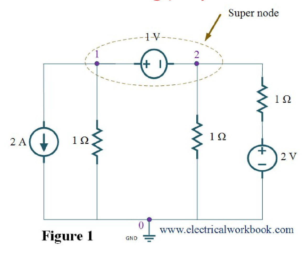
Super node-procedure

  • When a voltage source (independent or dependent) is connected between two non-reference nodes called supernode
  • Apply Kirchhoff's Current Law (KCL) (1st1^{\text{st}} statement
  • Current enter the node is equal to current leaving
  • Open circuit the shared voltage source and apply kcl both nodes

Page 130 of 185

Apply the rule current entering = current leaving(super node case)

Circuit diagram illustrating a super node case

Figure 1


Page 131 of 185

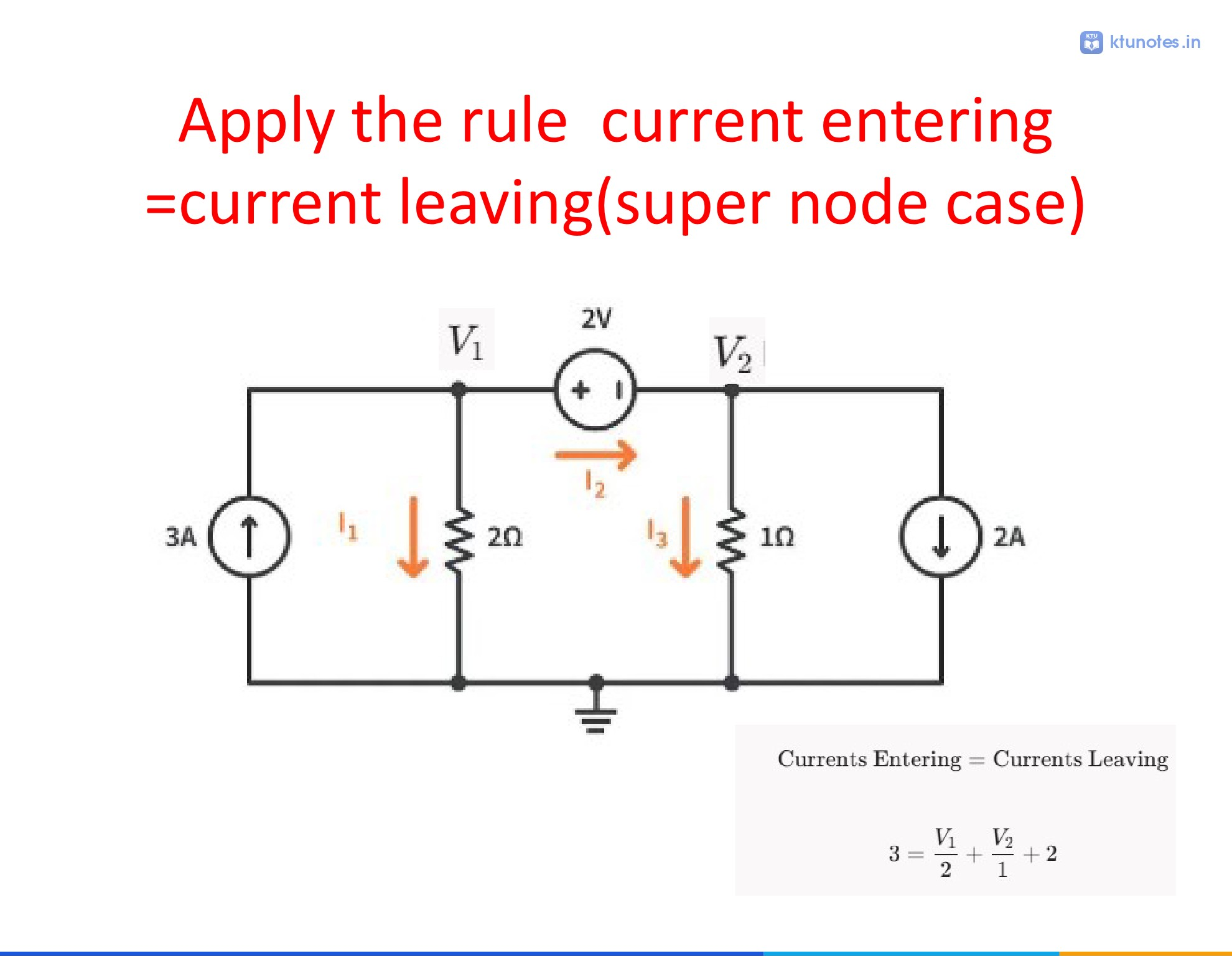
Apply the rule current entering = current leaving(super node case)

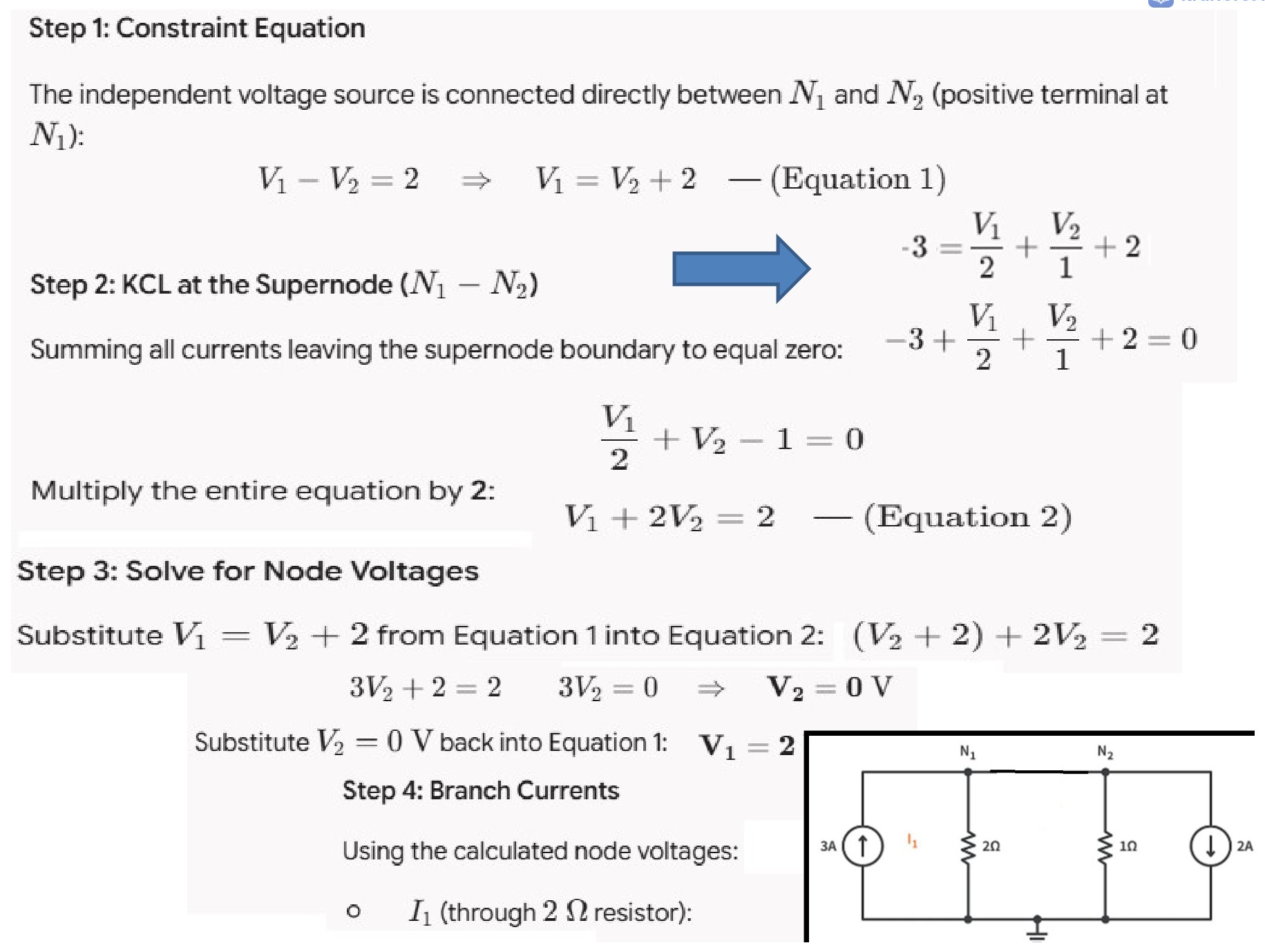
Circuit diagram showing a supernode with two voltage nodes V1 and V2, a 2V independent voltage source between them, resistors of 2 ohms and 1 ohm, current sources of 3A (upward) and 2A (downward), and branch currents I1, I2, I3.

Currents Entering=Currents Leaving\text{Currents Entering} = \text{Currents Leaving}

3=V12+V21+23 = \frac{V_1}{2} + \frac{V_2}{1} + 2


Page 132 of 185

[Non-content page]


Page 133 of 185

Step 1: Constraint Equation

The independent voltage source is connected directly between N1N_1 and N2N_2 (positive terminal at N1N_1): V1−V2=2  ⟹  V1=V2+2−(Equation 1)V_1 - V_2 = 2 \implies V_1 = V_2 + 2 - (\text{Equation 1})

-3 &= \frac{V_1}{2} + \frac{V_2}{1} + 2\\ -3 + \frac{V_1}{2} + \frac{V_2}{1} + 2 &= 0 \end{aligned}$ Step 2: KCL at the Supernode ($N_1 - N_2$) Summing all currents leaving the supernode boundary to equal zero: $\frac{V_1}{2} + V_2 - 1 = 0$ Multiply the entire equation by 2: $V_1 + 2V_2 = 2 - (\text{Equation 2})$ Step 3: Solve for Node Voltages Substitute $V_1 = V_2 + 2$ from Equation 1 into Equation 2: $(V_2 + 2) + 2V_2 = 2$ $3V_2 + 2 = 2 \quad 3V_2 = 0 \implies \mathbf{V_2 = 0\text{ V}}$ Substitute $V_2 = 0\text{ V}$ back into Equation 1: $\mathbf{V_1 = 2}$ Step 4: Branch Currents Using the calculated node voltages: * $I_1$ (through $2\text{ }\Omega$ resistor): ![Circuit diagram with nodes N1 and N2, a 3A current source, a 2 ohm resistor, a 1 ohm resistor, and a 2A current source.](/notes/cse/s1/electrical/module-1/assets/page-033-image-1-source.png) ---

Page 134 of 185

Apply the rule current entering = current leaving(super node case)

Circuit diagram illustrating a super node with voltage and current sources

Figure 1


Page 135 of 185

Step 1: Constraint Equation v1−v2=1v1=v2+1−(Equation 1)v_1 - v_2 = 1 \\[6pt] v_1 = v_2 + 1 \quad - (\text{Equation 1})

Step 2: KCL Equation at the Supernode (1−2)(1 - 2) Applying KCL (sum of all currents leaving the supernode boundary = 0):

2⏟from 2A source+v11⏟down 1Ω resistor+v21⏟down middle 1Ω resistor+v2−21⏟down right 1Ω branch=0\underbrace{2}_{\text{from } 2\text{A source}} + \underbrace{\frac{v_1}{1}}_{\text{down } 1\Omega \text{ resistor}} + \underbrace{\frac{v_2}{1}}_{\text{down middle } 1\Omega \text{ resistor}} + \underbrace{\frac{v_2 - 2}{1}}_{\text{down right } 1\Omega \text{ branch}} = 0

Step 3: Solve the System of Equations Substitute Equation 1 (v1=v2+1v_1 = v_2 + 1) into Equation 2: (v2+1)+2v2=0(v_2 + 1) + 2v_2 = 0 3v2+1=03v_2 + 1 = 0 3v2=−1  ⟹  v2=−13 V≈−0.333 V3v_2 = -1 \implies \mathbf{v_2 = -\frac{1}{3} \text{ V} \approx -0.333 \text{ V}}

Substitute v2=−13 Vv_2 = -\frac{1}{3} \text{ V} back into Equation 1: v1=−13+1  ⟹  v1=23 V≈0.667 Vv_1 = -\frac{1}{3} + 1 \implies \mathbf{v_1 = \frac{2}{3} \text{ V} \approx 0.667 \text{ V}}


Page 136 of 185

Apply the rule current entering = current leaving (super node case)

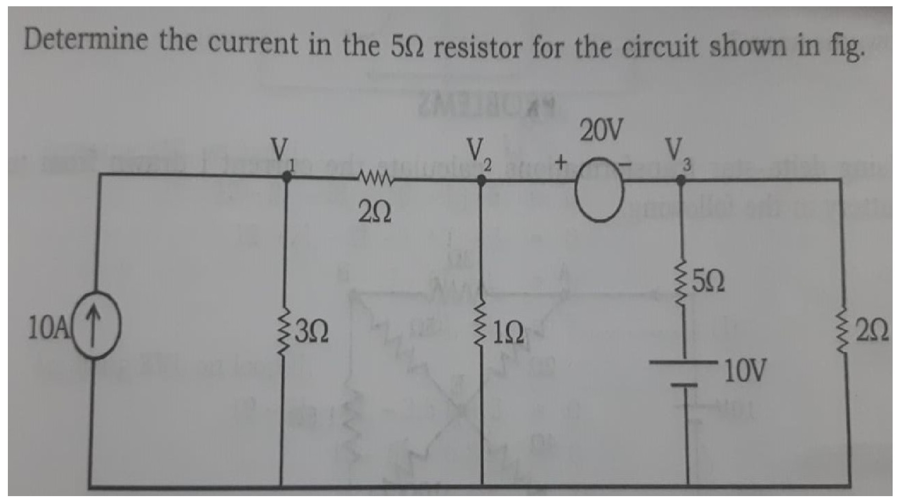
Determine the current in the 5 Ω5\,\Omega resistor for the circuit shown in fig.

Circuit diagram with nodes V1, V2, V3, a 10A current source, a 20V independent voltage source, and resistors of 2Ω, 3Ω, 1Ω, 5Ω, and 2Ω.


Page 137 of 185

V2−V3=20  ⟹  V2=V3+20V_2 - V_3 = 20 \implies V_2 = V_3 + 20

2. KCL at Node 1 (V1V_1)

Summing currents leaving node V1V_1: −10+V13+V1−V22=0-10 + \frac{V_1}{3} + \frac{V_1 - V_2}{2} = 0

3. KCL at the Supernode (2−32-3)

Summing all currents leaving the combined supernode 2−32-3: V2−V12+V21+V3−105+V32=0\frac{V_2 - V_1}{2} + \frac{V_2}{1} + \frac{V_3 - 10}{5} + \frac{V_3}{2} = 0


Page 138 of 185

  1. Calculate Current in the 5 Ω5\,\Omega Resistor

The 5 Ω5\,\Omega resistor is connected between node V3V_3 and the 10 V10\text{ V} source. The current I5 ΩI_{5\,\Omega} flowing downwards through the resistor is given by:

I5 Ω=V3−105I_{5\,\Omega} = \frac{V_3 - 10}{5}

Substitute V3=−8.421 VV_3 = -8.421\text{ V}:

I5 Ω=−8.421−105=−18.4215=−3.684 AI_{5\,\Omega} = \frac{-8.421 - 10}{5} = \frac{-18.421}{5} = -3.684\text{ A}


Page 139 of 185

equivalent resistance

Star --Delta Conversion

(Resistive network)

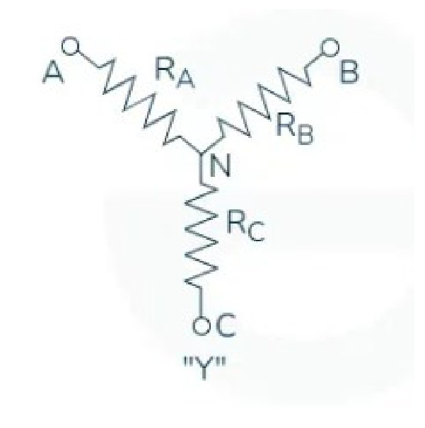
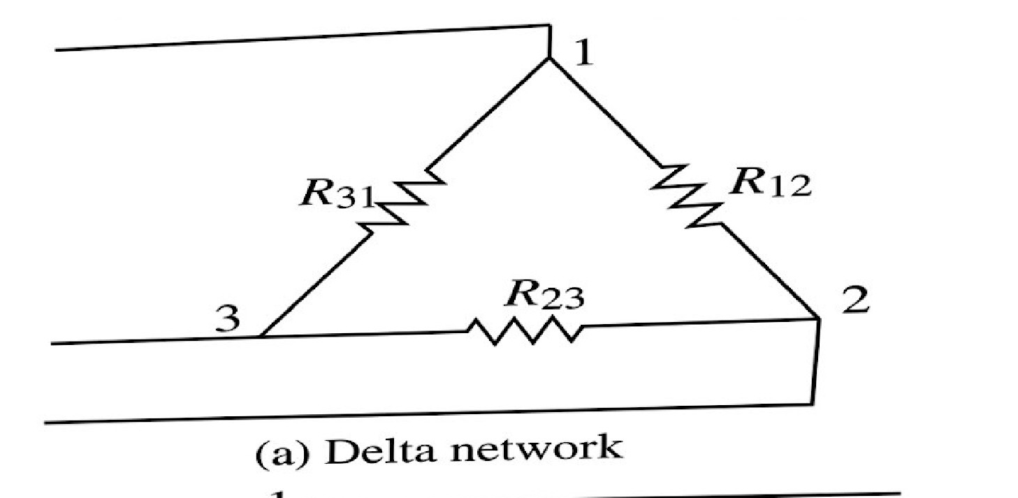
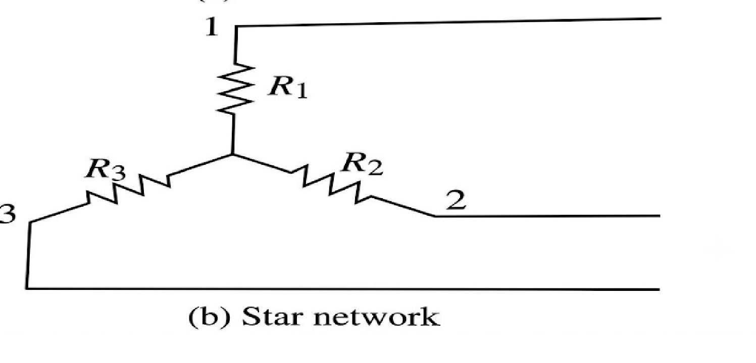
  • Star (Wye, Y) and Delta (Δ\Delta) are the two main ways to connect three-phase electrical loads or impedance networks

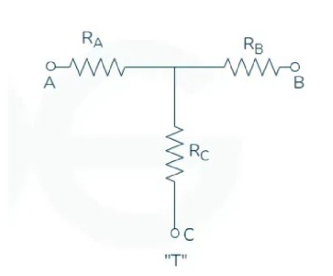
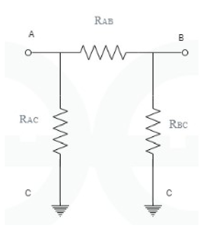
T-network circuit diagram

Y-network (Star) circuit diagram


Page 140 of 185

T-network circuit diagram with resistors R_AB, R_AC, R_BC and terminals A, B, C

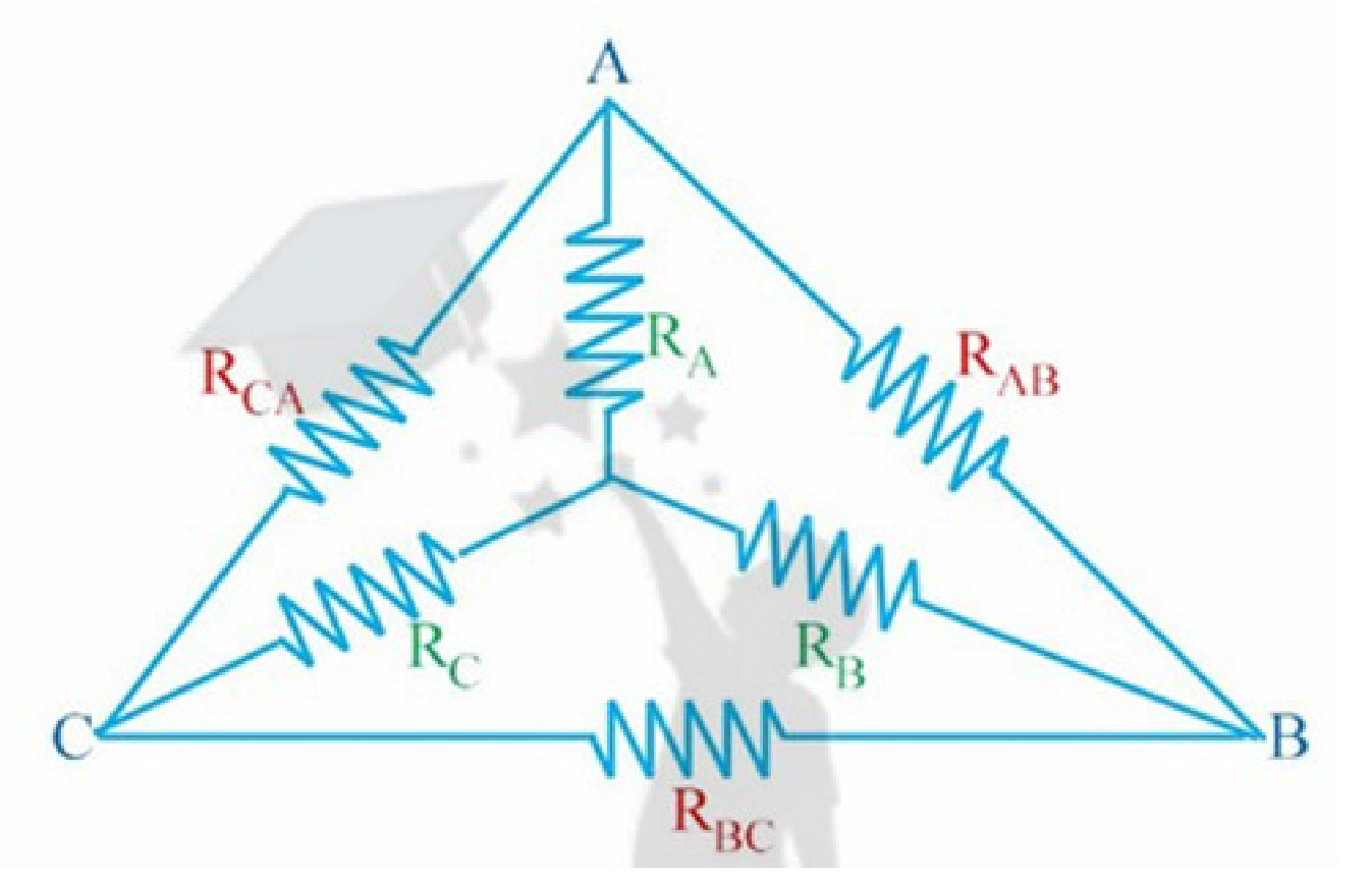
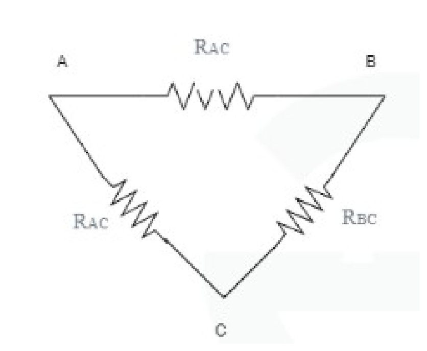
Delta network circuit diagram with resistors R_AC, R_BC, R_AB and terminals A, B, C forming a triangle


Page 141 of 185

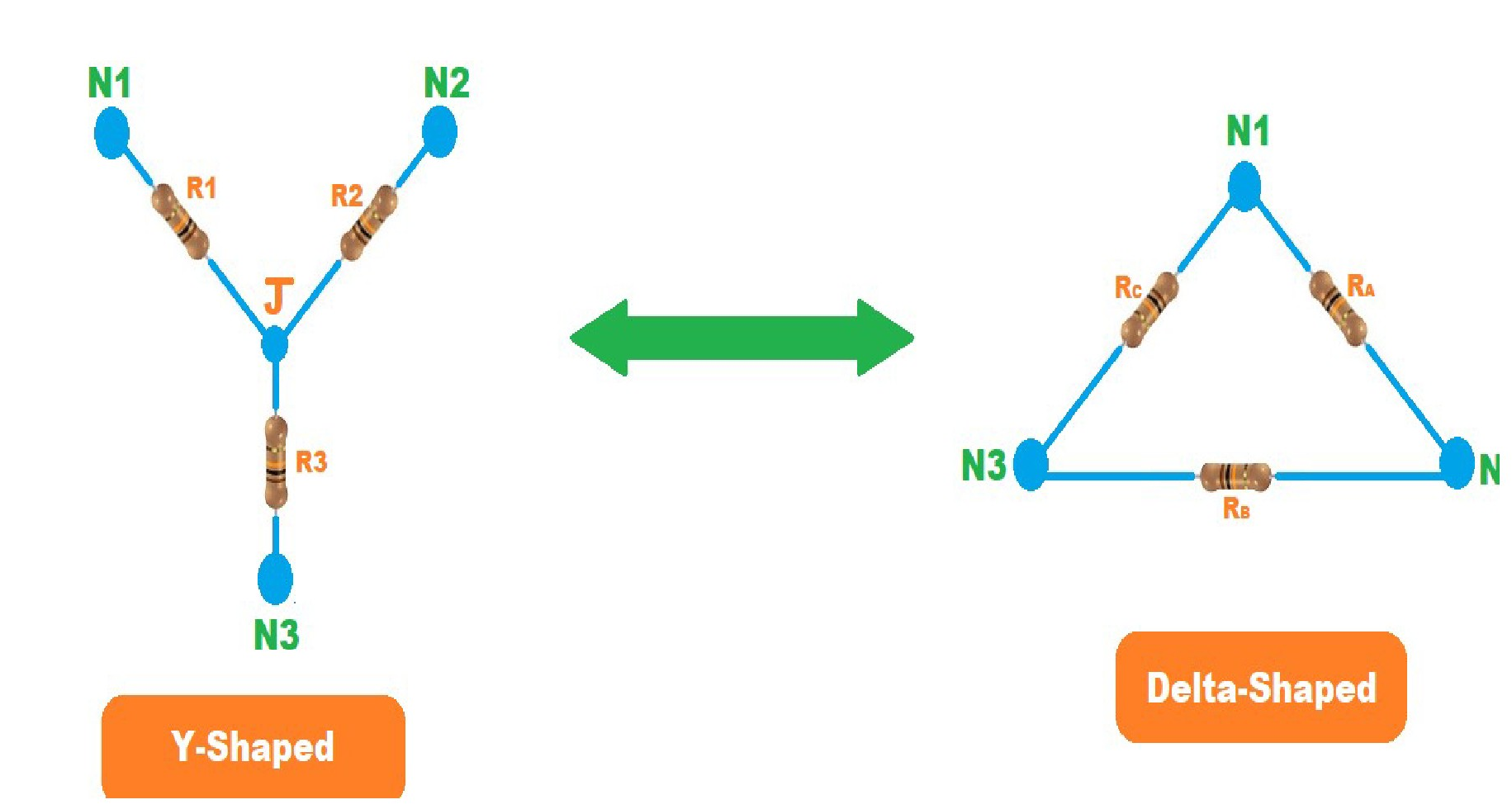
Y-Shaped to Delta-Shaped resistor conversion diagram


Page 142 of 185

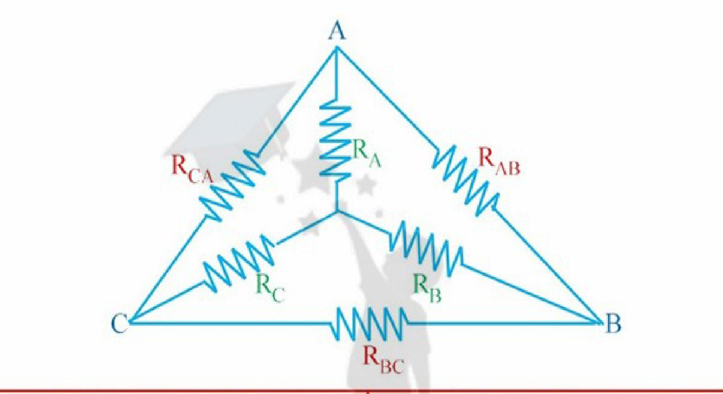
this electric circuit difficult to identify the total resistance

Electric circuit diagram showing delta-wye or triangle configuration with nodes A, B, C and resistors RA, RB, RC, RAB, RBC, RCA.


Page 143 of 185

Delta network circuit diagram

(a) Delta network

Star network circuit diagram

(b) Star network


Page 144 of 185

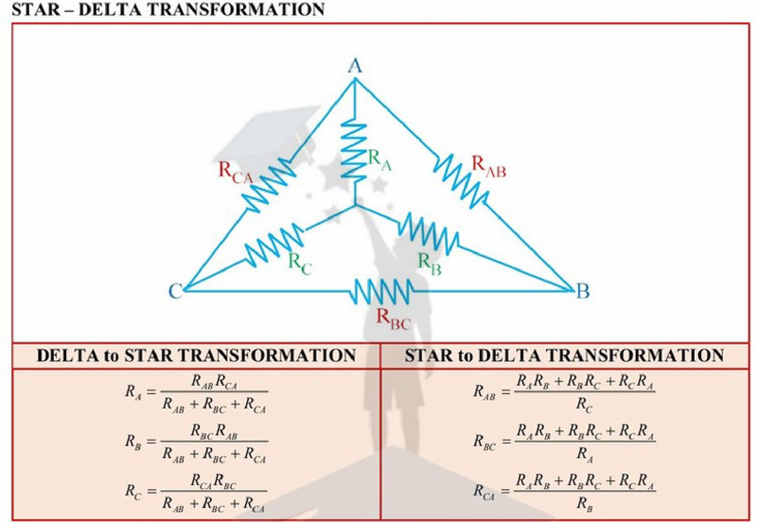
Star -- Delta Conversion (Resistive network)

STAR -- DELTA TRANSFORMATION

Star and Delta resistive network transformation diagram and formulas

DELTA to STAR TRANSFORMATION

RA=RABRCARAB+RBC+RCAR_A = \frac{R_{AB} R_{CA}}{R_{AB} + R_{BC} + R_{CA}}

RB=RBCRABRAB+RBC+RCAR_B = \frac{R_{BC} R_{AB}}{R_{AB} + R_{BC} + R_{CA}}

RC=RCARBCRAB+RBC+RCAR_C = \frac{R_{CA} R_{BC}}{R_{AB} + R_{BC} + R_{CA}}

STAR to DELTA TRANSFORMATION

RAB=RARB+RBRC+RCRARCR_{AB} = \frac{R_A R_B + R_B R_C + R_C R_A}{R_C}

RBC=RARB+RBRC+RCRARAR_{BC} = \frac{R_A R_B + R_B R_C + R_C R_A}{R_A}

RCA=RARB+RBRC+RCRARBR_{CA} = \frac{R_A R_B + R_B R_C + R_C R_A}{R_B}


Page 145 of 185

STAR -- DELTA TRANSFORMATION

Star and Delta network interconnected with nodes A, B, C and resistors R_A, R_B, R_C, R_AB, R_BC, R_CA

DELTA to STAR TRANSFORMATIONSTAR to DELTA TRANSFORMATION
RA=RABRCARAB+RBC+RCAR_A = \frac{R_{AB} R_{CA}}{R_{AB} + R_{BC} + R_{CA}}<br><br>RB=RBCRABRAB+RBC+RCAR_B = \frac{R_{BC} R_{AB}}{R_{AB} + R_{BC} + R_{CA}}<br><br>RC=RCARBCRAB+RBC+RCAR_C = \frac{R_{CA} R_{BC}}{R_{AB} + R_{BC} + R_{CA}}RAB=RARB+RBRC+RCRARCR_{AB} = \frac{R_A R_B + R_B R_C + R_C R_A}{R_C}<br><br>RBC=RARB+RBRC+RCRARAR_{BC} = \frac{R_A R_B + R_B R_C + R_C R_A}{R_A}<br><br>RCA=RARB+RBRC+RCRARBR_{CA} = \frac{R_A R_B + R_B R_C + R_C R_A}{R_B}

Page 146 of 185

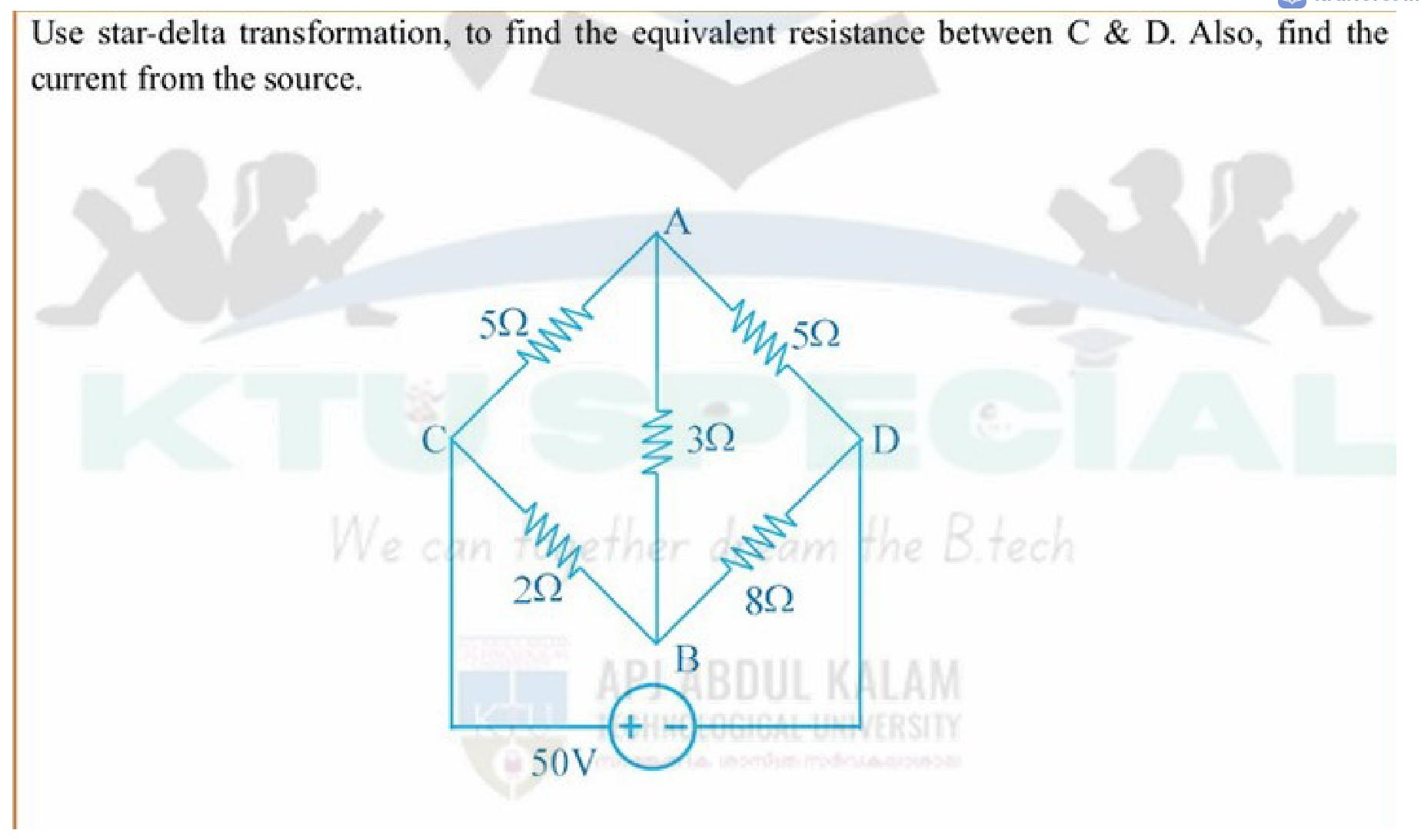
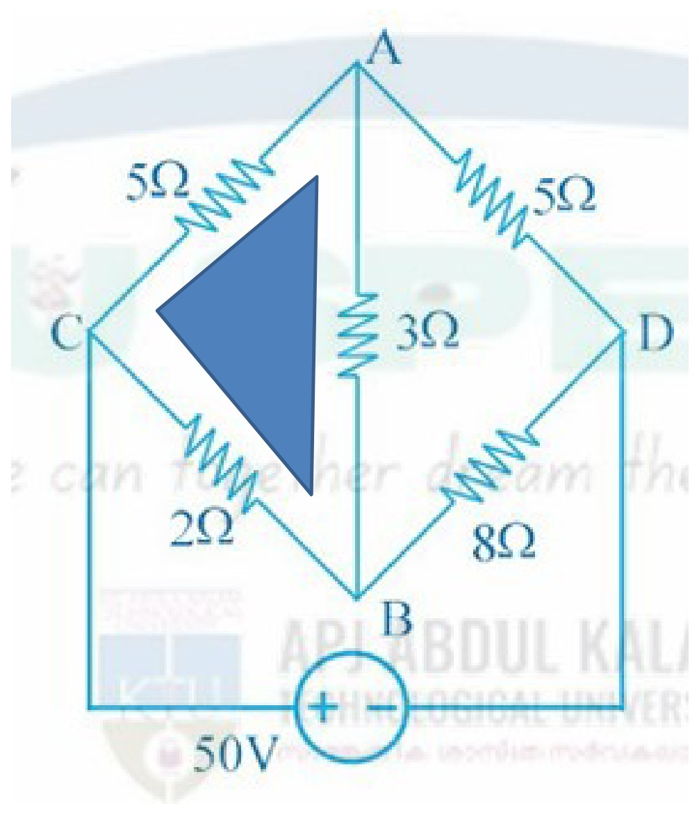
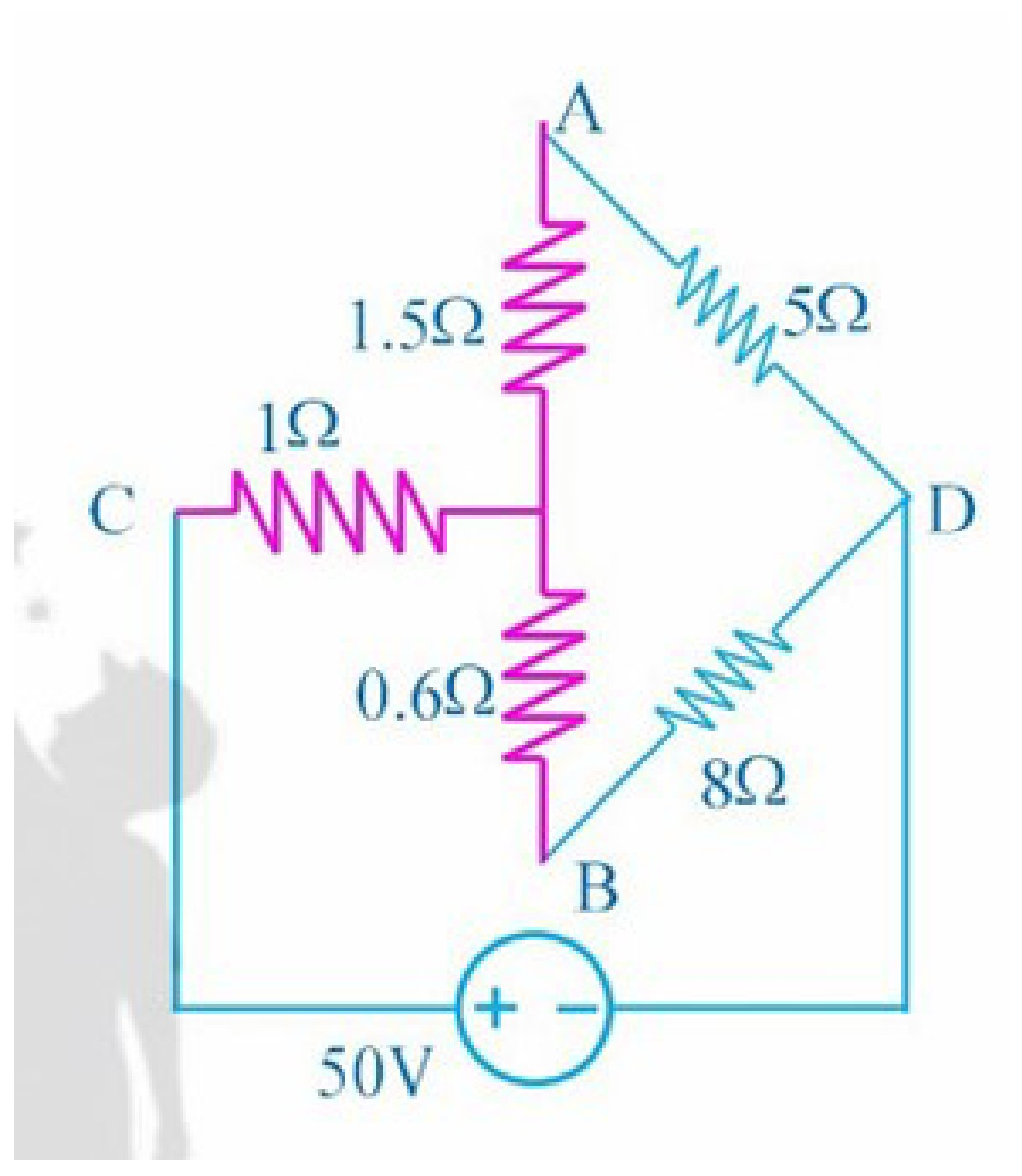
Use star-delta transformation, to find the equivalent resistance between C & D. Also, find the current from the source.

Bridge circuit with resistors and a 50V voltage source


Page 147 of 185

Electrical circuit diagram with a bridge configuration connected to a 50V voltage source


Page 148 of 185

RA=RABRCARAB+RBC+RCA=5×35+3+2=1.5 ΩR_A = \frac{R_{AB}R_{CA}}{R_{AB} + R_{BC} + R_{CA}} = \frac{5 \times 3}{5 + 3 + 2} = 1.5\,\Omega

RB=RBCRABRAB+RBC+RCA=3×25+3+2=0.6 ΩR_B = \frac{R_{BC}R_{AB}}{R_{AB} + R_{BC} + R_{CA}} = \frac{3 \times 2}{5 + 3 + 2} = 0.6\,\Omega

RC=RCARBCRAB+RBC+RCA=5×25+3+2=1 ΩR_C = \frac{R_{CA}R_{BC}}{R_{AB} + R_{BC} + R_{CA}} = \frac{5 \times 2}{5 + 3 + 2} = 1\,\Omega


Page 149 of 185

Electrical bridge circuit diagram with resistors and a DC voltage source


Page 150 of 185

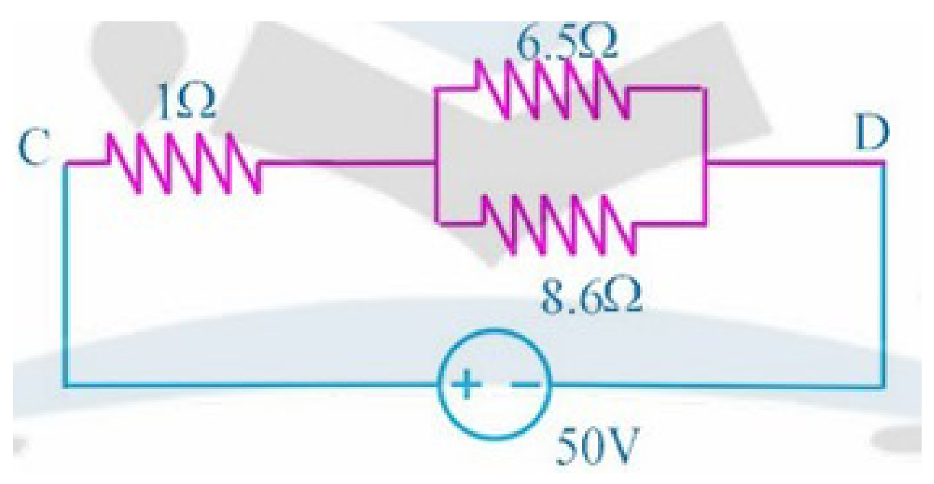
Circuit diagram with a 1 ohm resistor in series with a parallel combination of 6.5 ohm and 8.6 ohm resistors, connected to a 50V DC source.

Req=1+6.5×8.66.5+8.6=4.7ΩR_{eq} = 1 + \frac{6.5 \times 8.6}{6.5 + 8.6} = 4.7\Omega

Current drawn from the supply I=504.7=10.64 A\text{Current drawn from the supply } I = \frac{50}{4.7} = 10.64\text{ A}


Page 151 of 185

[Non-content page]


Page 152 of 185

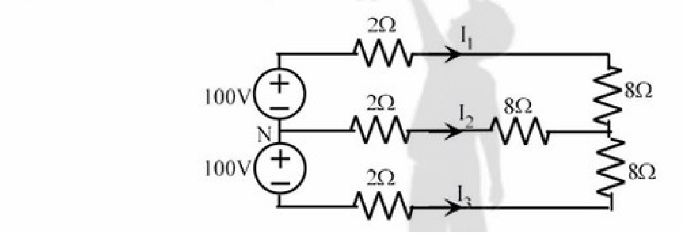
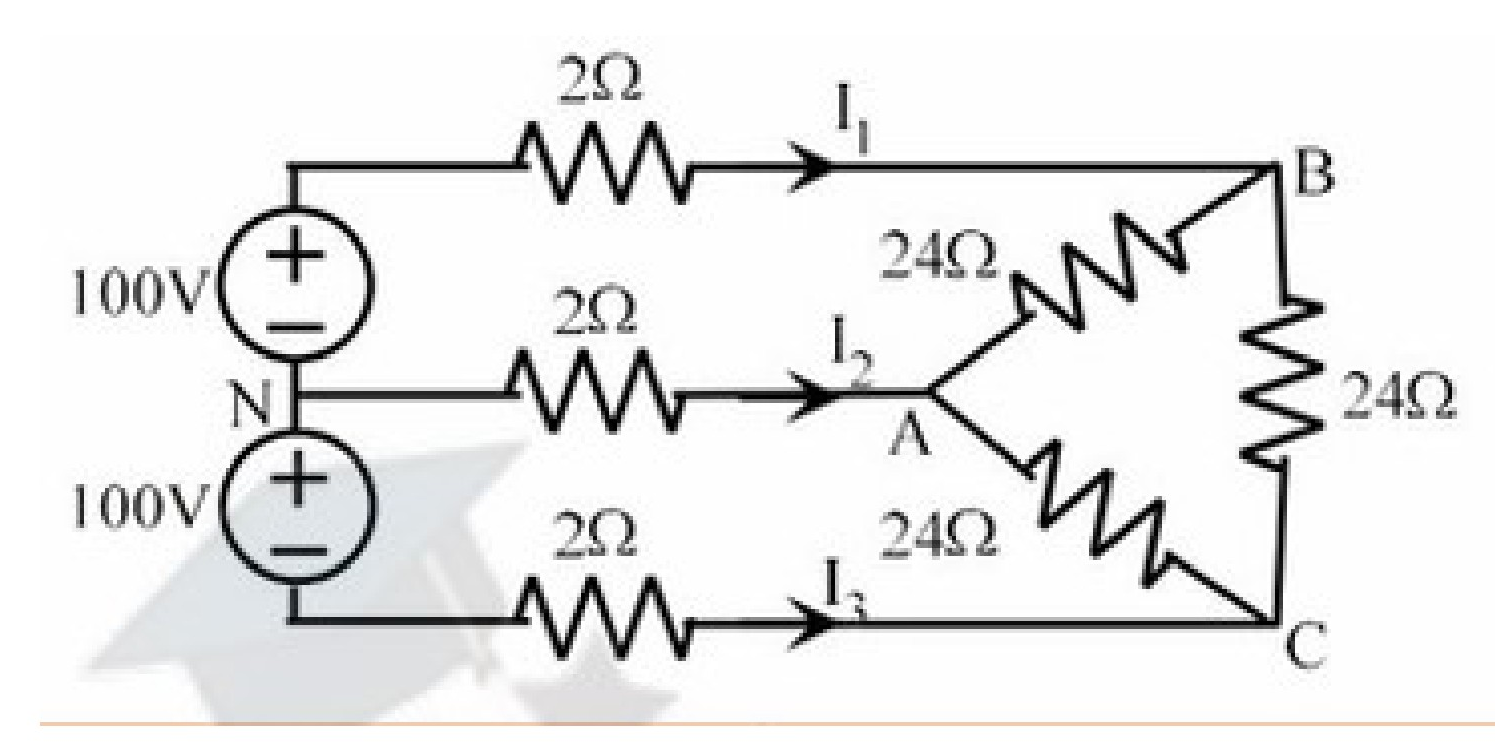
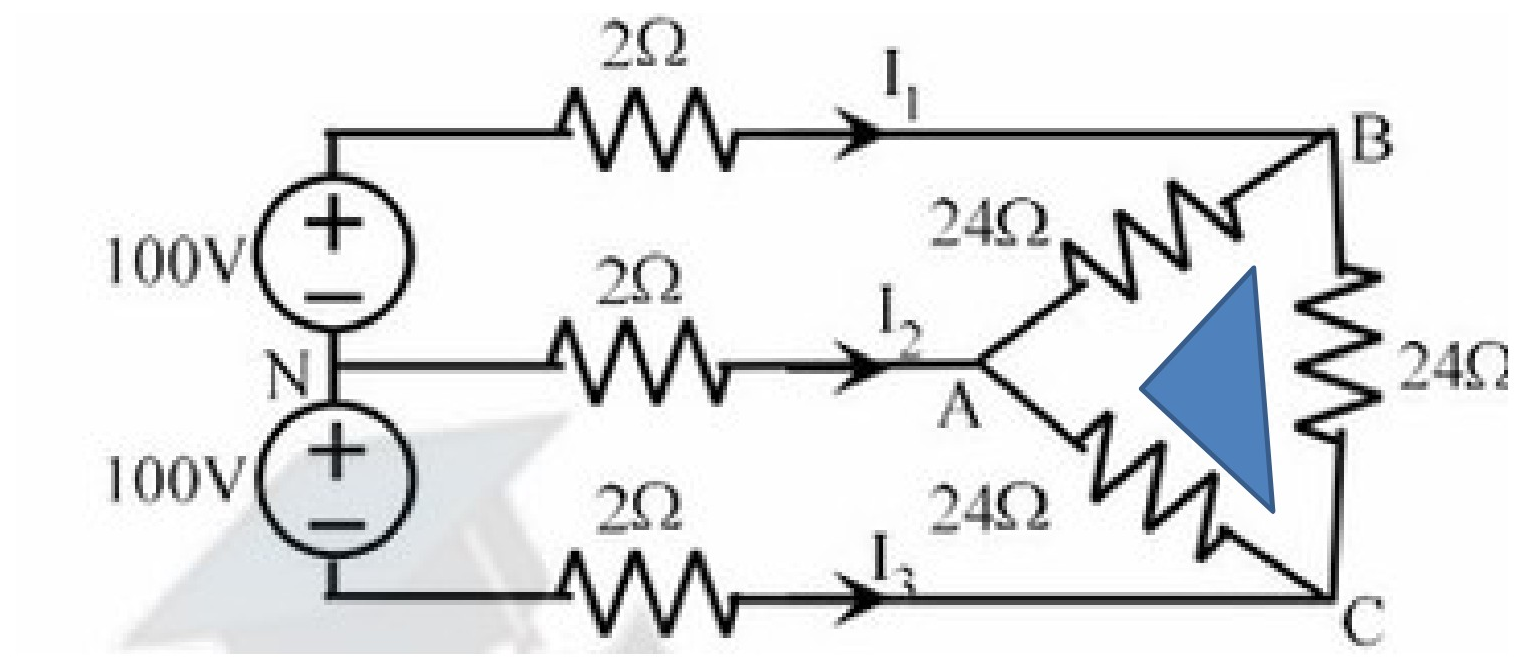
For the network shown in figure, determine the equivalent delta network using delta - star and star-delta transformations and hence find currents I1I_1, I2I_2 and I3I_3.

Electrical circuit diagram with three voltage sources, three series resistors, and a star-connected load network.


Page 153 of 185

An electrical circuit diagram with two 100V DC sources, three line resistors of 2Γ each, current indicators I1, I2, I3, and a delta-connected load of three 24Γ resistors between nodes A, B, and C.


Page 154 of 185

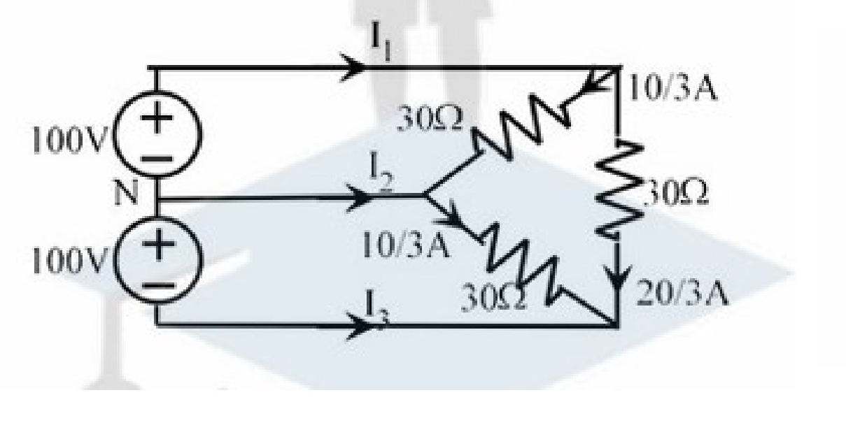
Using delta to star transformation,

Circuit diagram showing three-wire supply with 100V sources, 2 ohm resistors in each line, and load resistors of 8 ohms arranged in a bridge network.

Transformed circuit diagram showing a star-connected load with 30 ohm resistors and corresponding equations for currents I1, I2, and I3.

I_1 &= \frac{10}{3} + \frac{20}{3} = 10\text{ A} \\ I_2 &= \frac{10}{3} - \frac{10}{3} = 0 \\ I_3 &= -\frac{10}{3} - \frac{20}{3} = -10\text{ A} \end{aligned}$ ---

Page 155 of 185

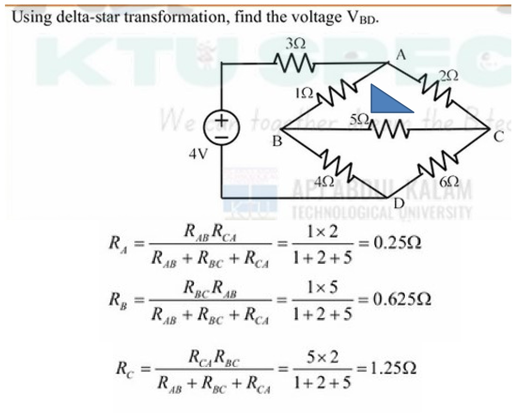
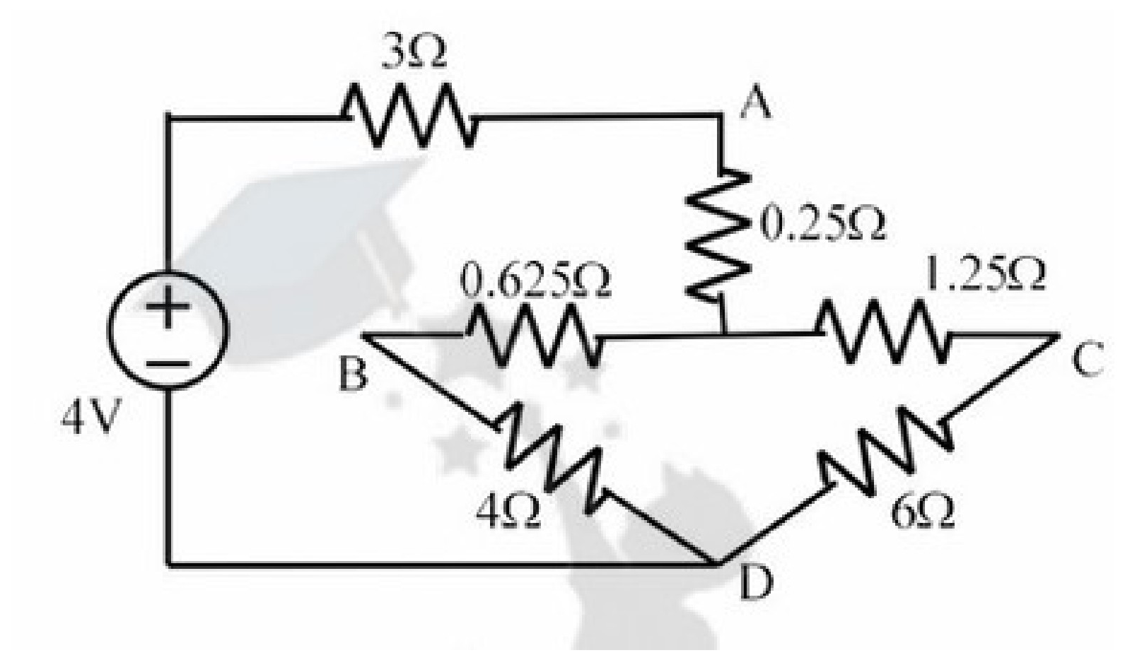
Using delta-star transformation, find the voltage VBDV_{BD}.

Circuit diagram containing a bridge network and a DC voltage source

RA=RABRCARAB+RBC+RCA=1×21+2+5=0.25ΩR_A = \frac{R_{AB} R_{CA}}{R_{AB} + R_{BC} + R_{CA}} = \frac{1 \times 2}{1 + 2 + 5} = 0.25\Omega

RB=RBCRABRAB+RBC+RCA=1×51+2+5=0.625ΩR_B = \frac{R_{BC} R_{AB}}{R_{AB} + R_{BC} + R_{CA}} = \frac{1 \times 5}{1 + 2 + 5} = 0.625\Omega

RC=RCARBCRAB+RBC+RCA=5×21+2+5=1.25ΩR_C = \frac{R_{CA} R_{BC}}{R_{AB} + R_{BC} + R_{CA}} = \frac{5 \times 2}{1 + 2 + 5} = 1.25\Omega


Page 156 of 185

Electrical circuit diagram with a 4V DC source and multiple resistors


Page 157 of 185

Current drawn from source, I=43+0.25+4.625×7.254.625+7.25=0.6586 AI = \dfrac{4}{3 + 0.25 + \dfrac{4.625 \times 7.25}{4.625 + 7.25}} = 0.6586\text{ A} \

Current through 4 Ω4\,\Omega resistance, I4 Ω=7.254.625+7.25×0.6586=0.402 AI_{4\,\Omega} = \dfrac{7.25}{4.625 + 7.25} \times 0.6586 = 0.402\text{ A} \

VBD=4×I4 Ω=4×0.402=1.608 VV_{BD} = 4 \times I_{4\,\Omega} = 4 \times 0.402 = 1.608\text{ V}


Page 158 of 185

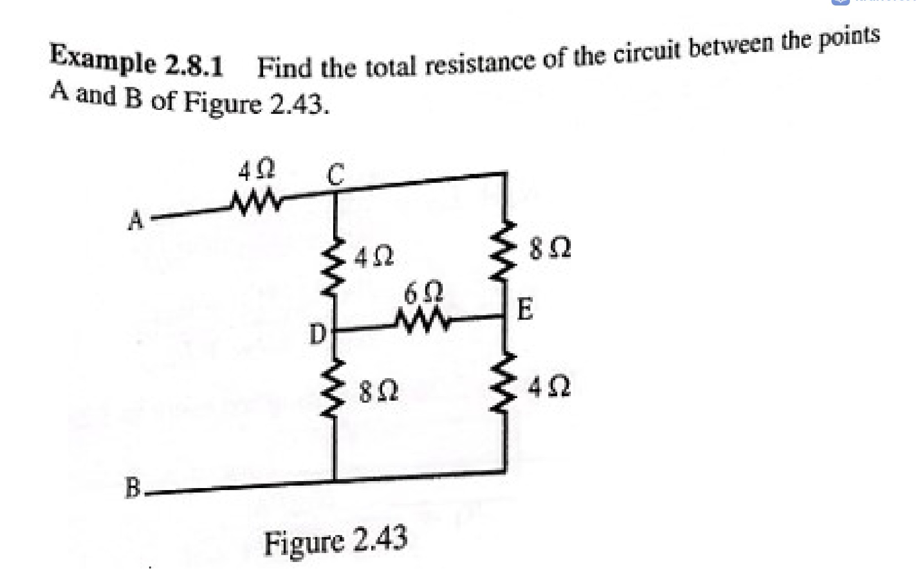
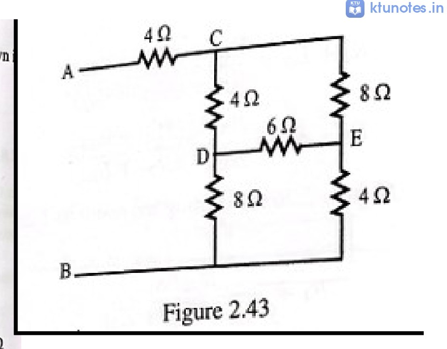
Example 2.8.1 Find the total resistance of the circuit between the points A and B of Figure 2.43.

Circuit diagram with resistors connected in series and parallel between points A and B

Figure 2.43


Page 159 of 185

Solution

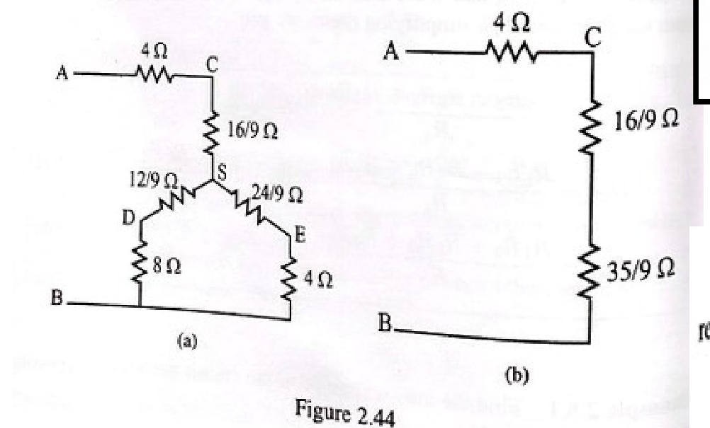
The delta CDE of Figure 2.43 is converted into equivalent star as shown in Figure 2.44(a).

RCS=8×418=169 ΩR_{CS} = \frac{8 \times 4}{18} = \frac{16}{9} \ \Omega

RES=8×618=249 ΩR_{ES} = \frac{8 \times 6}{18} = \frac{24}{9} \ \Omega

RDS=6×418=129 ΩR_{DS} = \frac{6 \times 4}{18} = \frac{12}{9} \ \Omega

Figure 2.44 showing delta to star conversion steps (a) and (b)

Figure 2.44

Figure 2.43 original bridge circuit

Figure 2.43

Blue arrow pointing right

Two parallel resistances between S and B can be simplified to a single resistance of 359 Ω\frac{35}{9} \ \Omega as

RSB=(129+8)∥(249+4)=359 ΩR_{SB} = \left(\frac{12}{9} + 8\right) \parallel \left(\frac{24}{9} + 4\right) = \frac{35}{9} \ \Omega

∴Total resistance, RAB=4+169+359=879 Ω\therefore \text{Total resistance, } R_{AB} = 4 + \frac{16}{9} + \frac{35}{9} = \frac{87}{9} \ \Omega


Page 160 of 185

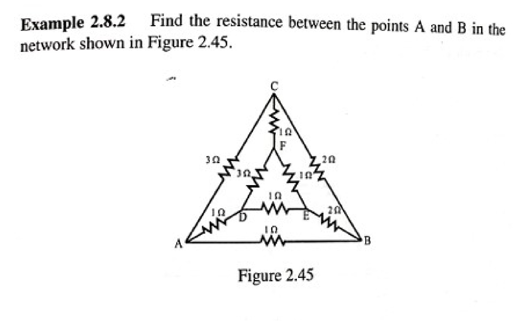
Example 2.8.2 Find the resistance between the points A and B in the network shown in Figure 2.45.\n\n

Resistor network diagram (Figure 2.45)

\n\nFigure 2.45


Page 161 of 185

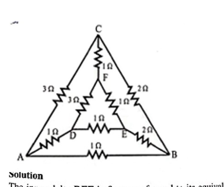
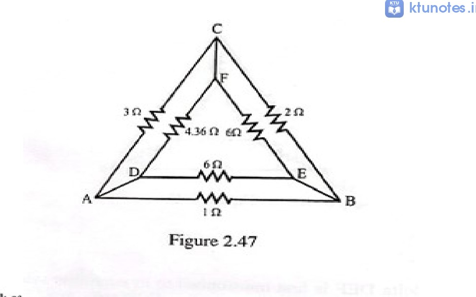
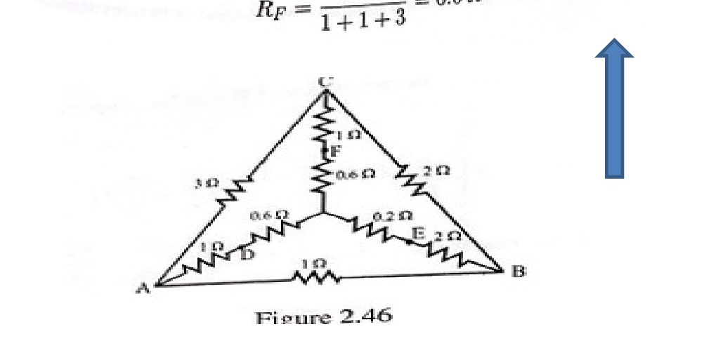
Circuit diagram of a bridge network with outer delta ABC and inner delta DEF

Circuit diagram for Figure 2.47

Solution

The inner delta DEFDEF is first transformed to its equivalent star network as given below.

RD=3×11+1+3=0.6  ΩR_D = \frac{3 \times 1}{1 + 1 + 3} = 0.6\;\Omega

RE=1×11+1+3=0.2  ΩR_E = \frac{1 \times 1}{1 + 1 + 3} = 0.2\;\Omega

RF=3×11+1+3=0.6  ΩR_F = \frac{3 \times 1}{1 + 1 + 3} = 0.6\;\Omega

Circuit diagram with star transformation, Figure 2.46

Arrow pointing upward

RFE=1.6+2.2+1.6×2.21.6=6  ΩR_{FE} = 1.6 + 2.2 + \frac{1.6 \times 2.2}{1.6} = 6\;\Omega

RDE=1.6+2.2+1.6×2.21.6=6  ΩR_{DE} = 1.6 + 2.2 + \frac{1.6 \times 2.2}{1.6} = 6\;\Omega

RFD=1.6+1.6+1.6×1.62=4.36  ΩR_{FD} = 1.6 + 1.6 + \frac{1.6 \times 1.6}{2} = 4.36\;\Omega

Resistances RABR_{AB}, RBCR_{BC} and RACR_{AC} are given by,

RAB=6×16+1=0.86  ΩR_{AB} = \frac{6 \times 1}{6 + 1} = 0.86\;\Omega

RBC=6×26+2=1.5  ΩR_{BC} = \frac{6 \times 2}{6 + 2} = 1.5\;\Omega

RAC=3×4.363+4.36=1.78  ΩR_{AC} = \frac{3 \times 4.36}{3 + 4.36} = 1.78\;\Omega

∴ Resistance across AB=(RAC+RBC)∥RAB\therefore \text{ Resistance across } AB = (R_{AC} + R_{BC}) \parallel R_{AB}

=(1.78+1.5)×0.8(1.78+1.5)+0.8=0.64  Ω= \frac{(1.78 + 1.5) \times 0.8}{(1.78 + 1.5) + 0.8} = 0.64\;\Omega


Page 162 of 185

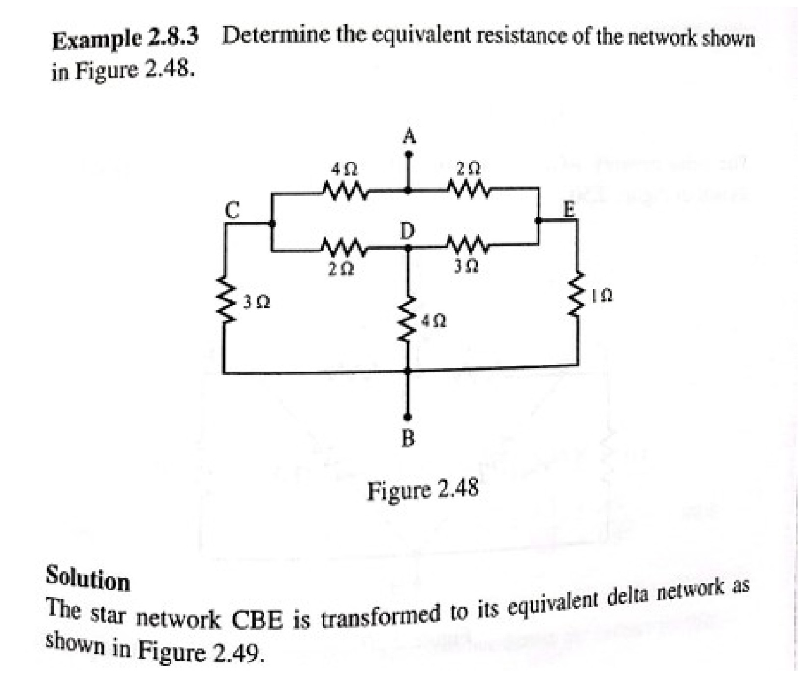
Example 2.8.3 Determine the equivalent resistance of the network shown in Figure 2.48.

Circuit diagram for Example 2.8.3 with resistors and terminals A and B

Figure 2.48

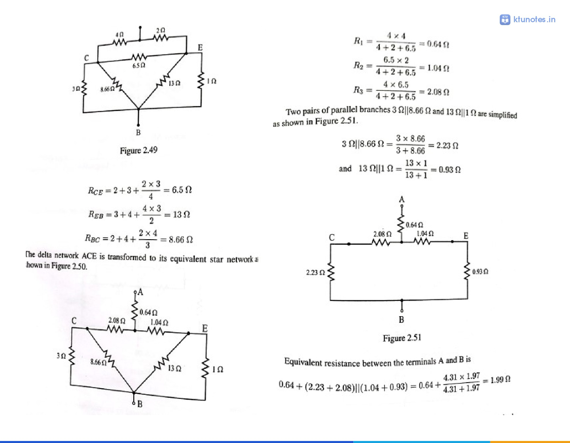
Solution The star network CBE is transformed to its equivalent delta network as shown in Figure 2.49.


Page 163 of 185

Circuit diagram Figure 2.49 showing a bridge network with resistors

Figure 2.49

R_{CE} &= 2 + 3 + \frac{2 \times 3}{4} = 6.5 \; \Omega \\ R_{EB} &= 3 + 4 + \frac{4 \times 3}{2} = 13 \; \Omega \\ R_{BC} &= 2 + 4 + \frac{2 \times 4}{3} = 8.66 \; \Omega \end{aligned}$ The delta network ACE is transformed to its equivalent star network as shown in Figure 2.50. ![Circuit diagram Figure 2.50 showing star-delta transformation](/notes/cse/s1/electrical/module-1/assets/page-063-image-2-source.png) Figure 2.50 $\begin{aligned} R_1 &= \frac{4 \times 4}{4 + 2 + 6.5} = 0.64 \; \Omega \\ R_2 &= \frac{6.5 \times 2}{4 + 2 + 6.5} = 1.04 \; \Omega \\ R_3 &= \frac{4 \times 6.5}{4 + 2 + 6.5} = 2.08 \; \Omega \end{aligned}$ Two pairs of parallel branches $3 \; \Omega \parallel 8.66 \; \Omega$ and $13 \; \Omega \parallel 1 \; \Omega$ are simplified as shown in Figure 2.51. $3 \; \Omega \parallel 8.66 \; \Omega = \frac{3 \times 8.66}{3 + 8.66} = 2.23 \; \Omega$ and $13 \; \Omega \parallel 1 \; \Omega = \frac{13 \times 1}{13 + 1} = 0.93 \; \Omega$ ![Circuit diagram Figure 2.51 showing simplified equivalent circuit](/notes/cse/s1/electrical/module-1/assets/page-063-image-3-source.png) Figure 2.51 Equivalent resistance between the terminals A and B is $0.64 + (2.23 + 2.08) \parallel (1.04 + 0.93) = 0.64 + \frac{4.31 \times 1.97}{4.31 + 1.97} = 1.99 \; \Omega$ ---

Page 164 of 185

Example 2.8.4 Find the equivalent resistance across the battery terminals

Bridge circuit with resistors and a battery


Page 165 of 185

in the bridge network shown in Figure 2.52

Bridge network with resistors connected in a diamond shape and a DC voltage source at the bottom.

Figure 2.52

Solution

The delta network DAC has been transformed to its equivalent star as shown in Figure 2.53.

R1=2×12+1+1=0.5 ΩR_1 = \frac{2 \times 1}{2 + 1 + 1} = 0.5\ \Omega

R2=1×12+1+1=0.25 ΩR_2 = \frac{1 \times 1}{2 + 1 + 1} = 0.25\ \Omega

R3=2×12+1+1=0.5 ΩR_3 = \frac{2 \times 1}{2 + 1 + 1} = 0.5\ \Omega

Equivalent circuit diagram after delta-to-star transformation.

Figure 2.53

Now the total resistance across the points D and B is

0.5+(0.25+1)∥(0.5+1)=0.5+1.25×1.51.25+1.5=1311 Ω0.5 + (0.25 + 1) \parallel (0.5 + 1) = 0.5 + \frac{1.25 \times 1.5}{1.25 + 1.5} = \frac{13}{11}\ \Omega

Battery symbol

Figure 2.52


Page 166 of 185

Example 2.8.5 Obtain a simplified delta network from the network shown in Figure 2.54.

Circuit diagram of a bridged delta-star network with nodes A, B, C, and D, and resistors of various values.

Figure 2.54


Page 167 of 185

Solution

The star in the Figure 2.54 is converted to delta and combined with the existing delta as shown in Figure 2.55(a).

Circuit conversion from star-delta to combined delta and simplified delta network

R_{AB} &= 6 + 4 + \frac{6 \times 4}{3} = 18\text{ }\Omega\\ R_{AC} &= 6 + 3 + \frac{6 \times 3}{4} = 13.5\text{ }\Omega\\ R_{BC} &= 4 + 3 + \frac{4 \times 3}{6} = 9\text{ }\Omega \end{aligned}$ The simplified delta network is shown in figure 2.55(b). ---

Page 168 of 185

Elementary concept of magnatic circuits (2nd2^{\text{nd}} half)

Magnetic Circuits: Basic Terminology: MMF, field strength, flux density, reluctance - Comparison between electric and magnetic circuits - Series and parallel magnetic circuits with composite materials (numerical problems not needed)


Page 169 of 185

[Non-content page]


Page 170 of 185

Magnetic Circuits

A material which possesses magnetic properties is called a magnet. A magnet attracts pieces of iron. When suspended freely, it points in the direction of North and South. The phenomenon by which this attraction takes place is called magnetism. There are two types of magnets available; permanent magnets and electromagnets.

The understanding of the concepts of magnetic circuits is essential for the design and analysis of electromagnetic devices such as transformers, generators and motors.

A magnetic field is created around a bar magnet. Figure 3.1 shows the magnetic lines of force around a bar magnet. The lines of magnetic field from a bar magnet form closed lines. By convention, the direction of magnetic field is taken to be outward from the North Pole and into the South Pole of the magnet.

Magnetic field around a bar magnet showing closed lines of force originating from the North (N) pole and entering the South (S) pole.

Figure 3.1: Magnetic field around a bar magnet


Page 171 of 185

3.3 Magnetic field around a current carrying conductor

Diagram of a straight vertical conductor carrying current I, surrounded by concentric circular magnetic field lines.

(b)


Page 172 of 185

3.4 Magnetic flux

The total number of magnetic lines of force in a magnetic field is called the magnetic flux. It is denoted by Φ\Phi and its unit is Weber.

The properties of magnetic flux are listed below.

  1. The magnetic flux lines are imaginary lines.
  2. Each line of magnetic flux forms a closed loop.
  3. Magnetic flux lines do not intersect each other.
  4. They behave like stretched elastic threads and always try to shorten themselves.
  5. The flux lines which are parallel and in same direction repel each other.

The magnetic flux lines always form closed paths. The closed path followed by the flux lines is called a magnetic circuit.


Page 173 of 185

3.5 Magnetic flux density

Magnetic flux density is the flux per unit area at right angles to the direction of the flux. If Φ\Phi is the flux and AA is the area of cross-section, then magnetic flux density denoted by BB is

B=ΦAB = \frac{\Phi}{A}

The unit of magnetic flux density is Wb/m2\text{Wb/m}^2 or Tesla.

3.6 Magneto motive force

Magneto Motive Force (MMF) is the force which establishes the magnetic flux in a magnetic circuit. When a current is passed through a coil, a magnetic flux is set up around it. The product of current (II) and number of turns (NN) of the coil gives mmf.

MMF, FF is given by the expression,

F=NIF = NI

Its unit is Ampere-Turns (AT).


Page 174 of 185

3.7 Magnetic field intensity

Magnetic field intensity is the magneto motive force per unit length of the magnetic circuit. It is denoted by HH and its unit is Ampere-Turns/meter. Magnetic field intensity is also called magnetic field strength or magnetizing force.

H=mmfl=FlH = \frac{\text{mmf}}{l} = \frac{F}{l}

H=NIlH = \frac{NI}{l}

Or, F=NI=HlF = NI = Hl \dots(3.1)

3.8 Permeability

The ability of a material to conduct magnetic flux through it is called permeability of that material. It is represented by the letter μ\mu and the unit is Henry/meter. The flux and hence the flux density BB are directly proportional to the magnetizing force HH.

i.e.,

B∝HB \propto H

B=μHB = \mu H (3.2)

μ=BH\mu = \frac{B}{H} (3.3)

where μ\mu is the constant of proportionality and is called permeability of the magnetic material. Permeability of free space is denoted by μo\mu_o and μo=4π×10−7\mu_o = 4\pi \times 10^{-7} Henry/meter.


Page 175 of 185

3.9 Relative permeability

When the mmf is applied to ferromagnetic materials, the flux produced is very large when compared with that in air, vacuum or nonmagnetic material. The ratio of the flux density produced in a material to the flux density produced in vacuum by the same magnetizing force is called relative permeability of that material. It is denoted by μr\mu_r.

i.e., μr=Flux density produced in a materialFlux density in vacuum\text{i.e., } \mu_r = \frac{\text{Flux density produced in a material}}{\text{Flux density in vacuum}}

Also,

μr=μμ0\mu_r = \frac{\mu}{\mu_0}

The expression 3.2 can be rewritten as, B=μ0μrHB = \mu_0 \mu_r H


Page 176 of 185

3.10 Reluctance

Reluctance of a material is its property of opposing the creation of magnetic flux in it. Reluctance is denoted by SS and is directly proportional to the length and inversely proportional to the area of cross-section of the magnetic path. It is analogous to resistance in an electrical circuit.

i.e.,

S∝lAS \propto \frac{l}{A}

\boxed{S = \frac{l}{\mu_0 \mu_r A}} \tag{3.4}

where

l=mean length of magnetic circuit in meterl = \text{mean length of magnetic circuit in meter} A=area of cross-section of magnetic circuit in m2A = \text{area of cross-section of magnetic circuit in } m^2 μ0=permeability of free space=4π×10−7 Henry/meter\mu_0 = \text{permeability of free space} = 4\pi \times 10^{-7} \text{ Henry/meter} μr=relative permeability of magnetic material\mu_r = \text{relative permeability of magnetic material}

Thus the reluctance is dependent on physical dimensions and the material of the magnetic circuit.

Also,

Reluctance=mmfFlux\text{Reluctance} = \frac{\text{mmf}}{\text{Flux}}

i.e., S=FΦS = \frac{F}{\Phi}

From the expressions 3.1 and 3.2,

F=Hl=Bμ0μrl=ΦAμ0μrlsince B=ΦAF = Hl = \frac{B}{\mu_0 \mu_r} l = \frac{\Phi}{A \mu_0 \mu_r} l \quad \text{since } B = \frac{\Phi}{A}

From equation 3.4, F=SΦF = S\Phi

i.e., mmf=Reluctance×Flux (3.5)\text{mmf} = \text{Reluctance} \times \text{Flux} \text{ (3.5)}

Reluctance, S=FΦ=NIΦ=HlΦ\boxed{\text{Reluctance, } S = \frac{F}{\Phi} = \frac{NI}{\Phi} = \frac{Hl}{\Phi}}

The unit of reluctance is Ampere-Turn per Weber (AT/Wb).


Page 177 of 185

3.11 Comparison of electric and magnetic circuits

Electric and magnetic circuits have many similarities. Tables 3.1 and 3.2 give comparison between electric and magnetic circuits.

Sl. No.Electric circuitMagnetic circuit

Electric circuit diagram showing a closed loop with a DC voltage source E, a resistor R, and current I flowing clockwise.

|

Magnetic circuit diagram showing a magnetic core wrapped with a coil carrying current I, producing flux Phi.

| | 1 | The closed path for electric current is called electric circuit. | The closed path for magnetic flux is called magnetic circuit. | | 2 | The cause of current flow is emf. | The cause of generation of flux is mmf. | | 3 | Opposition to flow of current is offered by resistance RR. | Opposition to flow of flux is offered by reluctance SS. | | 4 | Current, I=emfResistanceI = \frac{\text{emf}}{\text{Resistance}} expressed in amperes. | Flux, Φ=mmfReluctance\Phi = \frac{\text{mmf}}{\text{Reluctance}} expressed in webers. | | 5 | Electromotive force expressed in volts. | Magneto motive force expressed in Ampere-Turns. | | 6 | Current density, J=IAJ = \frac{I}{A} expressed in A/m2A/m^2. | Flux density, B=ΦAB = \frac{\Phi}{A} expressed in Wb/m2Wb/m^2 | | 7 | Resistance, R=lσAR = \frac{l}{\sigma A} where σ\sigma is the conductivity. | Reluctance, S=lμAS = \frac{l}{\mu A} where μ\mu is permeability. |


Page 178 of 185

Differences between electric and magnetic circuits

No.Electric circuitMagnetic circuit
1Electric current actually flows in the circuit.Magnetic flux is a field quantity; it does not physically flow like electric charge.
2Energy is required as long as current flows in a resistive circuit.Energy is required to establish the magnetic field. The source comparison idealizes maintenance of a steady field; coil resistance can still consume power.
3At constant temperature, the resistance is constant for an ohmic conductor.Reluctance can depend on flux density because the material permeability changes.
4Good electrical insulators can confine current to a defined path.Magnetic flux cannot be perfectly confined; some leakage flux remains.

Page 179 of 185

3.17.1 Series magnetic circuit

Consider a simple magnetic circuit shown in Figure 3.7. It consists of a coil of NN turns wound over a single core material having uniform cross-sectional area AA and mean length of flux path ll. mmf is indicated by NINI which is equal to HlHl. It is represented by F\mathcal{F}. Reluctance offered by the circuit to the flow of flux is denoted as SS in its electrical equivalent representation. This is useful for simplifying analysis of magnetic circuit even though there is no physical connection between winding and core.

Diagram showing a physical magnetic core with a coil and its electrical equivalent circuit

Figure 3.7: Simple magnetic circuit

Polarity of mmf is determined based on the direction of flux. Here it is in clock wise direction as indicated in figure. mmf source is expressed by NINI and mmf drops are expressed by HlHl, where HH is the magnetizing force on a section of a magnetic circuit and ll is the length of the section.


Page 180 of 185

Magnetic circuit with air gap and its equivalent electrical/magnetic circuit diagram

an air gap of length lgl_g. Thus there are two mediums in the magnetic circuit namely (a) iron and (b) air. Magnetic flux is same through these mediums and thus it is a series magnetic circuit. Also total reluctance of the circuit is the sum of reluctances of iron and air.

Taking,

Number of turns =N= N

Current through the coil (exciting current) =I= I (A)

Mean length of the flux path through iron =li= l_i (m)

Length of the flux path through air gap =lg= l_g (m)

Cross-sectional area =A= A (m2\text{m}^2)

Magnetic flux density =B= B (Wb/m2\text{Wb}/\text{m}^2)

Permeability of iron =μi= \mu_i (Henry/m2\text{Henry}/\text{m}^2)

Reluctance of iron =Si= \mathcal{S}_i (AT/Wb\text{AT}/\text{Wb})

Reluctance of air gap =Sg= \mathcal{S}_g (AT/Wb\text{AT}/\text{Wb})

We can develop equations for this magnetic circuit as

Total mmf in the circuit,

NI=Hili+HglgNI = H_i l_i + H_g l_g

Magnetic field intensity required for iron, Hi=Bμ0μiH_i = \dfrac{B}{\mu_0 \mu_i}

Magnetic field intensity required for air, Hg=Bμ0H_g = \dfrac{B}{\mu_0}

Therefore,

NI=Hili+HglgNI = H_i l_i + H_g l_g

Derivation steps for the total mmf and flux in a magnetic circuit with an air gap


Page 181 of 185

why this air gap?

An air gap (lgl_g) is intentional in magnetic cores (like inductors, flyback transformers, and DC-biased systems) to control magnetic flux and prevent core saturation.

  • Prevents Core Saturation: High magnetic permeability in iron cores means they saturate quickly under high current or DC bias. The air gap acts as high magnetic reluctance, flattening the B-H curve so the core can handle higher currents without saturating.

  • Stores Magnetic Energy: Ferromagnetic core materials hold very little energy, whereas air stores significant magnetic energy. The air gap serves as the primary energy storage region in devices like inductors and flyback transformers (W=12 ⋅ B2μ0 ⋅ VgapW = \frac{1}{2} \text{ }\text{·}\text{ } \frac{B^2}{\mu_0} \text{ }\text{·}\text{ } V_{\text{gap}}).

  • Stabilizes Inductance: An air gap makes total circuit reluctance dominated by the gap length rather than fluctuations in core permeability (μr\mu_r), keeping inductance (LL) stable across temperature changes and varying operating currents.

  • Linearizes the Magnetic Circuit: Air has a completely linear B-H response, reducing harmonic distortion in signal-processing inductors and audio transformers.


Page 182 of 185

3.17.2 Series-parallel magnetic circuits

Now consider a parallel magnetic circuit in which a coil of NN turns is wound on an iron core as shown in Figure 3.12.

For analyzing it, we draw its equivalent electrical representation as indicated in Figure 3.13.

Figure 3.12: A series-parallel magnetic circuit showing an iron core with a coil of N turns and magnetic flux paths.

Figure 3.12: A series-parallel magnetic circuit

Figure 3.13: Electrical equivalent circuit of series-parallel magnetic circuit.

Electrical equivalent circuit of series-parallel magnetic circuit


Page 183 of 185

We usually refer vertical links of core as limbs and horizontal links as yoke. In the figure AFAF, BEBE and CDCD are the limbs whereas ABAB, BCBC, FEFE and EDED are the yokes.

When the coil carries a current II in the direction shown, a magnetic flux Φ1\Phi_1 will be created in the first limb (AFAF) which will be in the upward direction. Flux Φ1\Phi_1 will be same along the yoke ABAB. At point BB, there are two parallel paths for flux. Thus Φ1\Phi_1 will be split into two components Φ2\Phi_2 and Φ3\Phi_3 such that Φ1=Φ2+Φ3\Phi_1 = \Phi_2 + \Phi_3, Φ2\Phi_2 along the central limb BEBE and Φ3\Phi_3 along the yoke BCBC. Values of Φ1\Phi_1 and Φ2\Phi_2 depend on respective reluctances of the paths. Φ2\Phi_2 and Φ3\Phi_3 again recombine at point EE and completes the path.

Total flux, Φ1=Φ2+Φ3\text{Total flux, } \Phi_1 = \Phi_2 + \Phi_3

Total mmf required=mmf for path EFAB+mmf for path BE or path BCDE\text{Total mmf required} = \text{mmf for path EFAB} + \text{mmf for path BE or path BCDE}

NI=Φ1S1+Φ2S2=Φ1S1+Φ3S3NI = \Phi_1 S_1 + \Phi_2 S_2 = \Phi_1 S_1 + \Phi_3 S_3

Some other forms of series-parallel magnetic circuits and their electric equivalent representations are shown below.


Page 184 of 185

Magnetic core (a) with Gap a and Gap b and its magnetic circuit equivalent (b)

Figure 3.14: A series-parallel magnetic circuit and its electric-equivalent representation

Magnetic core with two windows and two windings (a)

Magnetic core with center gap and side gap (a) and its equivalent magnetic circuit (b)

Magnetic circuit equivalent with two mmf sources and two loops

series-parallel magnetic circuit and its electric-equivalent
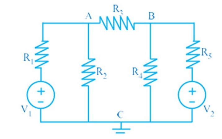

Page 185 of 185

[Non-content page]