
Page 1 of 18
Module 3 at a glance
Module 1 classified materials by their band gap: conductors (bands overlap), insulators (large gap) and, in between, semiconductors. This module studies this middle class in detail, and also the device on which all modern electronics is built, the p-n junction.
The story has two halves.
- Counting carriers. How many free electrons and holes does a semiconductor have at a given temperature? We derive the electron density in the conduction band and the hole density in the valence band, combine them to get the intrinsic carrier concentration, and see what doping and temperature do to the number of carriers and to the Fermi level.
- Joining p and n. When a p-type region and an n-type region are joined, a depletion region and a potential barrier are created. Biasing changes this barrier, and the result is the diode equation and the V-I characteristic of the diode.
Everything in the second half depends on the first half. The diode equation is really a statement about how the number of electrons on each side of a barrier depends on the height of that barrier, and the carrier-density formulas tell us exactly that.
KTU syllabus. Intrinsic semiconductor, derivation of density of electrons in conduction band and density of holes in valence band, intrinsic carrier concentration, variation of intrinsic carrier concentration with temperature, extrinsic semiconductor (qualitative). Formation of p-n junction, Fermi level in semiconductors (intrinsic and extrinsic), energy band diagram of p-n junction, qualitative description of charge flow across a p-n junction, forward and reverse biased p-n junctions, diode equation (derivation), I-V characteristics of p-n junction.
What you will be able to do
- Explain how holes are formed and why they behave as positive carriers.
- Explain what effective mass and density of states mean, and why both are needed to count carriers.
- Derive and , and give the physical reason for each step.
- Derive the intrinsic carrier concentration, state the law of mass action, and explain how depends on temperature and band gap.
- Describe n-type and p-type semiconductors with band diagrams, and describe how their carrier density changes over a wide range of temperature.
- Find the position of the Fermi level in intrinsic, n-type and p-type material, and explain why it moves with doping and temperature.
- Explain the formation of a p-n junction in terms of diffusion and drift, draw its band diagram, and explain what forward and reverse bias do.
- Derive the diode equation and draw and explain the V-I characteristic.
- Solve the standard numerical problems on , band gap and diode current, and a few more on doped carrier densities and conductivity.
How to use these notes
- Each topic is a page: idea → derivation or explanation → worked example → common mistakes.
- Green boxes show key ideas. Amber boxes marked Watch out show mistakes that make you lose marks. Boxes marked Note on the source show where the lecture notes were corrected. Boxes marked Beyond the syllabus give short extra points that make the syllabus topics easier to understand. They are not usually asked in exams on their own.
- The derivations of , , , the intrinsic Fermi level and the diode equation are favourite long-answer questions. Learn the steps and the reason for each step, not just the results.
- The last three pages have the standard numerical problems, extra worked examples, and practice questions with a formula sheet.
Where each topic sits
| Part | Pages |
|---|---|
| Intrinsic semiconductors | Holes, effective mass, density of states, electrons in the conduction band, holes in the valence band, intrinsic carrier concentration |
| Doping | Extrinsic semiconductors, carrier densities in doped material, Fermi level, conductivity |
| The p-n junction | Forming a junction, biasing, the diode equation, V-I characteristics |
| Practice | Numerical problems, more worked examples, practice and formula sheet |
Before you start. From Module 1: energy bands, the band gap , the Fermi-Dirac function , and conductivity . From maths: integration by substitution, and the laws of exponents and logarithms. Remember that at , because almost every estimate in this module compares an energy with .
Page 2 of 18
Intrinsic semiconductors and holes
The idea
An intrinsic semiconductor is a pure semiconductor, with no important impurities. Silicon (Si) and germanium (Ge) are the standard examples. Both belong to group IV of the periodic table. Each atom has four valence electrons, and in the crystal each atom shares one electron with each of its four nearest neighbours. These shared pairs are covalent bonds, and every valence electron is held in one of them.
At every valence electron is held in its bond. In terms of bands, the valence band is completely full and the conduction band is completely empty. A full band cannot carry current (for every electron moving in one direction there is another moving in the opposite direction, and there is no empty state to move into), and an empty band has nothing to carry. So at absolute zero a pure semiconductor is an insulator.
As the temperature rises, the lattice vibrates and some electrons get enough thermal energy to break their covalent bond. The energy needed is the band gap: about for silicon and for germanium. A freed electron moves almost freely through the spaces between the atoms. It has become a conduction electron. In terms of bands, the electron has jumped from the valence band to the conduction band.
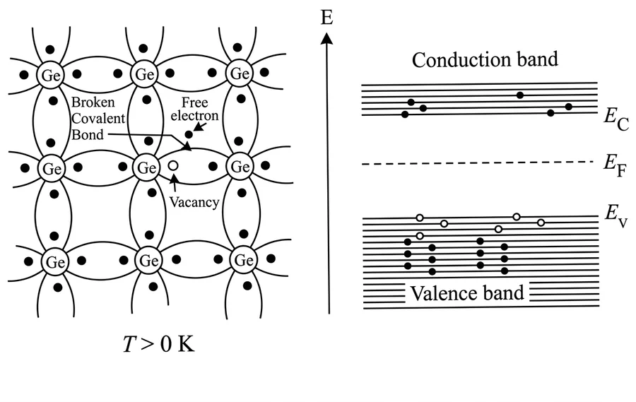
Thermal energy is shared randomly, so at room temperature () only a tiny fraction of bonds are broken at any moment. That is why the result depends so strongly on temperature, and why the number of carriers depends exponentially on .
Holes
When an electron leaves the valence band, it leaves behind an empty state in the bond it came from, called a hole.
- Why a hole acts as a positive charge. Before the bond broke, the region around it was electrically neutral: the negative charge of the electrons exactly balanced the positive nuclei. When one electron is removed, a net charge of is left at that place. So the hole is a "missing negative charge", which behaves in every electrical way like a positive charge .
- Why a hole can move. A valence electron in a neighbouring bond needs very little energy to hop into the vacancy, because it moves from one valence-band state to another of almost the same energy. When it does this, the vacancy appears where that electron came from. If this is repeated, the vacancy moves through the crystal. In an electric field, the valence electrons hop mostly against the field, so the hole moves with the field, opposite to the electrons, exactly as a positive charge would.
- Why holes count as carriers. The current produced by all those valence electrons hopping in one direction is the same as the current produced by a single positive particle moving in the other direction. It is much simpler to follow one hole than many electrons, so we treat holes as real charge carriers in the valence band.
A useful picture is a row of cars in a car park with one empty space. As each car moves forward into the space in front, the empty space moves backwards. Watching the space is easier than watching every car.
Key idea. Breaking one covalent bond creates an electron-hole pair. In an intrinsic semiconductor the number of free electrons is always equal to the number of holes, .
Generation, recombination and equilibrium
Two processes go on all the time:
- Generation: thermal energy breaks bonds and creates electron-hole pairs.
- Recombination: a conduction electron meets a hole and falls back into the bond, and both carriers disappear. The energy is released as heat (in silicon and germanium) or light (in materials such as GaAs, used in LEDs).
At a fixed temperature, the two rates become equal and the carrier numbers become steady. This is thermal equilibrium. If the temperature is raised, the generation rate increases, so the equilibrium carrier numbers also increase.
Properties of intrinsic semiconductors
| Property | Description |
|---|---|
| Pure form | a single semiconductor material (such as Si or Ge) with no intentional impurities |
| Equal carriers | at thermal equilibrium, the number of free electrons equals the number of holes |
| Conductivity | poor at room temperature, because only a tiny fraction of bonds are broken |
| Band gap | small: Si , Ge |
| Temperature dependence | heating creates more electron-hole pairs, so the conductivity rises steeply (negative temperature coefficient of resistance) |
| Two kinds of carrier | electrons in the conduction band and holes in the valence band both carry current |
Limitations
- The conductivity at room temperature is low.
- The current depends much more on temperature than on the applied voltage, so the behaviour of the device changes as the temperature changes.
- The conductivity cannot be chosen. It is fixed by the material and the temperature.
- So pure semiconductors are of little use in devices until they are doped (page 8).
Watch out. A hole is not a particle that "exists" on its own. It is a convenient way to describe the movement of many valence electrons into an empty state. Draw it as an open circle in the valence band, never in the conduction band. Also remember that the hole moves opposite to the electrons that fill it.
Page 3 of 18
Effective mass
To count carriers and to describe how they move, we need to know how an electron in a crystal responds to a force. The answer is the effective mass.
Why the ordinary mass is not enough
For a free body, Newton's second law gives the acceleration produced by a force :
This is correct only if is the only force acting. An electron in a crystal is not free. It moves through the periodic potential of the positive ion cores, which push and pull it differently at every point of the lattice. When we apply an external force (for example from an electric field), the actual acceleration of the electron is the combined result of the external force and all the internal crystal forces.
We have two choices:
- keep the true mass and add up all the internal forces (very complicated), or
- keep only the external force and include the effect of the crystal in a modified mass.
The second choice gives
where is the effective mass. It is the mass the electron appears to have when it responds to an external force inside that particular band of that particular crystal.
What determines the effective mass
The effective mass depends on the shape of the band near the energy where the carriers are. In quantum mechanics it is decided by how the energy of a state changes with its wave vector :
A sharply curved band gives a small effective mass (the carrier is easy to accelerate); a flat band gives a large one. You do not need this formula for the exam, but it explains the next two facts.
- In the conduction band, near its bottom , the band curves upwards like . The curvature is positive, so the effective mass of the electron is positive. Depending on the material, it can be smaller or larger than the free-electron mass . For example, it is about in silicon (for conduction) and in gallium arsenide.
- Near the top of the valence band the band curves downwards. The curvature is negative, so an electron there has a negative effective mass: an external force would make it accelerate opposite to the force. Physically, the crystal forces are stronger than the applied force for these electrons.
Why we use holes in the valence band
Negative-mass electrons are difficult to think about. But the valence band near its top is almost full, with only a few empty states. Describing the motion of the few holes is equivalent to describing the motion of all the valence electrons, and a hole near the top of the valence band behaves like a particle with
- positive charge , and
- positive effective mass .
Two negatives (negative charge, negative mass) make a positive description that follows Newton's law in the normal way. So we write for the effective mass of conduction electrons and for the effective mass of holes, and both are positive numbers.
Key idea. Effective mass is not a change in the electron itself. It is a bookkeeping trick that lets us use for a carrier inside a crystal, with all the crystal forces hidden inside .
Note on the source. The lecture notes said that the conduction-band effective mass "can be equal to or greater than" the free electron mass. In fact it is often smaller (as the examples show). What matters is that it is a property of the band, not of the electron itself.
Watch out. Do not write "the hole has negative mass". It is the valence-band electron near the band top that has a negative effective mass. The hole has a positive effective mass .
Page 4 of 18
Density of states
The idea
To find how many electrons are in the conduction band, we need two things for every energy :
- how many states (places for an electron) are there at that energy, and
- the probability that each state is occupied.
The second is the Fermi-Dirac function from Module 1. The first is the density of states.
In a band, the allowed energy levels are so close together (Module 1: about apart) that we treat them as continuous. Instead of counting individual levels, we ask: how many states per unit volume are there in a small energy range around ? This number is written , and is the density of states.
Density of states. The number of energy states per unit volume with energy between and is
where is the effective mass of the carriers, is Planck's constant, and is measured from the edge of the band.
Where the formula comes from (outline)
You are not asked to derive this, but the outline shows why each factor is there.
- A carrier in a crystal of volume behaves like a particle in a box. Its allowed momenta form a fine grid in "momentum space", with one state for each volume of that space.
- States with momentum between and fill a thin spherical shell of volume . Dividing by gives the number of states. Dividing by gives the number per unit volume.
- Each state can hold two electrons of opposite spin, which gives a factor .
- Finally, change from momentum to energy using , so and . Putting everything together gives the above.
What it tells us
- : there are no states exactly at the band edge, and there are more and more states as you go deeper into the band. The shell in momentum space becomes larger as you go to larger momentum.
- A larger effective mass gives more states at a given energy (the factor ). Flat bands are "dense" in states.
- In the conduction band, energy is measured up from , so is replaced by :
- In the valence band, hole energy is measured down from , so is replaced by :
Inside the band gap there are no states at all in a pure crystal, so there.
How it is used
The number of electrons in a small energy range is
and the total is the integral of this over the band. The next two pages carry out that integral for electrons and for holes.
Watch out. The formula uses the effective mass: in the conduction band and in the valence band. Writing the free electron mass is a common mistake. Also, in the formula is the energy measured from the band edge, not the absolute energy.
Page 5 of 18
Density of electrons in the conduction band
Plan
The number of electrons per unit volume in a small energy range is
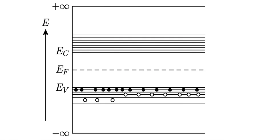
Then add up (integrate) over the whole conduction band, from its bottom to . The upper limit is not literally the top of the band. It is used because, as we will see, the occupation probability falls so fast with energy that states more than a few above contribute nothing, and extending the integral to infinity makes it easy to calculate without changing the answer.
Step 1: the two ingredients
Let be the number of electrons per unit volume with energy between and :
Number of states. Measuring energy from the band edge (the lowest energy a conduction electron can have):
Probability of occupation. The Fermi-Dirac function is
Why we may simplify it. In a semiconductor, the Fermi level lies in the gap, typically several tenths of an eV below . For every energy in the conduction band, is therefore at least that large, which is many times ( at room temperature). For example, if (mid-gap silicon), then even at the band edge and . Compared with that, the in the denominator is completely negligible:
This is the Boltzmann approximation: the electrons in the conduction band are so few, and so thinly spread over the available states, that the Pauli exclusion principle (which the in the Fermi-Dirac function represents) hardly matters, and they behave like a classical gas.
Note on the source. The lecture notes said " for all ". The approximation is really a condition. It is true when the Fermi level is several below the conduction band (a non-degenerate semiconductor), which is the normal case. It fails for very heavily doped material, where the Fermi level can reach or enter the band.
Step 2: set up the integral
Multiply the two ingredients and integrate over the band:
Take the constants outside. Split . The first factor does not depend on :
Step 3: substitute
The integrand depends on the energy above the band edge, so we use that as the new variable. Let , so and . The limits and become and . Then , and the constant factor joins outside:
Step 4: the standard integral
With this gives , so
Now simplify the constants: , since and .
Result
Meaning of
The constant
is called the effective density of states in the conduction band. The result reads as if all the conduction band states were squeezed into a single level at holding states per unit volume, each occupied with the Boltzmann probability . For silicon at it is about (). Note that itself depends on temperature, as , because at higher temperature the electrons spread over a wider slice of the band.
Key idea. The electron density depends exponentially on how far the Fermi level lies below the conduction band. If moves up by , increases by a factor . If it moves up by (about ), increases tenfold.
Note on the source. One place in the lecture notes wrote the standard integral as . The correct form is . The two are the same only when .
Watch out. Be careful with the sign in the exponent: , so is negative and is a small fraction of . The final factor and the power both come from the algebra in step 4. Show that working in the exam.
Page 6 of 18
Density of holes in the valence band
The method is like the electron derivation, with two changes: the states are in the valence band, and we need the probability that a state is empty (holds a hole) instead of full.
Step 1: the two ingredients
Let be the number of holes per unit volume with energy between and :
Number of states. Hole energies lie below the top of the valence band , so measure from downwards. plays the same role for holes that plays for electrons: it is the edge of the band where the carriers collect.
Probability that a state holds a hole. A hole is the absence of an electron. A state is either occupied (probability ) or empty (probability ), and these must add up to one, so
Why we may simplify it. In the valence band by several , so is large and negative, and . The term in the denominator is negligible compared with :
This is the same Boltzmann approximation, now for holes: very few valence states are empty, so holes also behave like a thin classical gas.
Step 2: set up the integral
Holes occupy energies from deep in the band up to . As for electrons, we take the lower limit as , because states more than a few below are almost certainly full and give no holes:
Step 3: substitute
Let , the depth below the band top in units of . Then , and . The limits and become and :
The minus sign reverses the limits, and joins the other constants:
Step 4: the standard integral
With , , so
Result
where
is the effective density of states in the valence band. It has the same meaning as : the result is as if all the valence band states were concentrated at . Because holes usually have a different effective mass from electrons, differs from (for silicon against ).
Key idea. The two results are mirror images. Electrons: exponent , the distance from up to the conduction band. Holes: exponent , the distance from down to the valence band. If the Fermi level moves up, increases and decreases by the same factor.
Watch out. Use , not , for holes. Remember that the effective mass changes to , the band edge to , and the order inside the exponent to .
Page 7 of 18
Intrinsic carrier concentration
The idea
In a pure semiconductor, every broken bond makes one electron and one hole, so
where is the intrinsic carrier concentration (or intrinsic carrier density). It is the number of electrons (or holes) per unit volume in the pure material at a given temperature.
Derivation
Since , we can write . Using the product is the trick: it removes the Fermi level, which we do not yet know. Multiply the two results of the last two pages:
Combine the prefactors: , and , leaving .
Combine the exponents: . The terms cancel:
Taking the square root:
Why depends only on and
The Fermi level has cancelled out completely. This makes physical sense: in a pure crystal, the number of broken bonds is decided by how much energy it costs to break one () and how much thermal energy is available (), together with the number of states available to receive the carriers ( and , which depend on the effective masses and on ). Nothing else about the crystal comes in.
Law of mass action
The product does not depend on :
So at a given temperature, for a given semiconductor, the product of the electron and hole densities is a constant. This is the law of mass action, named by analogy with chemistry, where the product of the concentrations of the reacting substances is fixed at equilibrium. Here the "reaction" is
Generation runs at a rate decided by the temperature, and recombination runs at a rate proportional to (an electron has to meet a hole). At equilibrium the two rates are equal, so is fixed.
The law holds for intrinsic and extrinsic semiconductors, because the derivation never assumed until the very end. If doping increases , more electrons are available to recombine with holes, so must fall until is back to . Page 9 uses this to find the minority carrier density in doped material.
How varies
- is independent of the Fermi level.
- decreases as the band gap increases, exponentially. A material with a wider gap has far fewer intrinsic carriers.
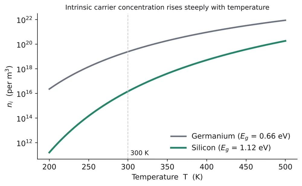
- increases steeply with temperature: . Both factors increase with , but the exponential completely dominates. The factor changes by only a few per cent over the range where changes by orders of magnitude.
- The factor in shows that breaking one bond produces two carriers: the energy cost is shared between the electron and the hole.
At room temperature, for silicon and for germanium. The smaller gap of germanium gives it over a thousand times more intrinsic carriers. Compare these with the roughly atoms per cubic metre in the crystal: in silicon at room temperature, with two bonds per atom, only about one bond in is broken.
A straight-line test
Taking logarithms of :
So a graph of against is a straight line of slope . Measuring the conductivity of a pure sample at several temperatures and plotting it in this way is a standard laboratory method to find the band gap.
Watch out. The exponent in is , with a 2. In or alone it is the distance to the band edge over , with no 2. Also, since the curve rises exponentially, heating by a few degrees changes a lot (see problem 1 on the numerical problems page: a rise roughly doubles in silicon).
Page 8 of 18
Extrinsic semiconductors
Doping
Adding a controlled amount of impurity to an intrinsic semiconductor is called doping. The impurity is the dopant, and the result is an extrinsic semiconductor.
The dopants come from group V (pentavalent, 5 valence electrons) or group III (trivalent, 3 valence electrons). Their atoms are about the same size as silicon and germanium atoms, so they take the place of host atoms in the crystal (substitutional impurities) without disturbing it much. Very small amounts are enough. A typical doping of dopant atoms per is only one dopant for every five million silicon atoms, yet it increases the carrier density about a million times above the intrinsic value.
Depending on the dopant, two types of extrinsic semiconductor are possible: n-type and p-type. Compared with intrinsic material, extrinsic semiconductors
- conduct much better,
- have a conductivity that can be fixed by choosing the doping concentration, and
- have a conductivity that depends much less on temperature over the normal working range (see the temperature regions below).
n-type semiconductors
Dopant: a pentavalent impurity such as phosphorus, arsenic or antimony.
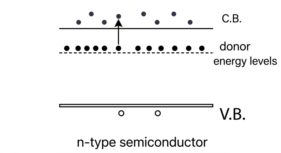
- Four of the five valence electrons form covalent bonds with four neighbouring silicon atoms. The fifth electron has no bond to join. It is held only weakly by the electrostatic attraction of its parent ion, and this attraction is further weakened by the surrounding crystal (its dielectric constant is about 12 in silicon). Its ionisation energy is only about to , compared with to break a bond.
- At ordinary temperatures, thermal energy easily frees this electron and it moves into the conduction band. It leaves behind a fixed positive ion (for example ), bound in the lattice and unable to move. Because the impurity atom donates an electron for conduction, it is called a donor.
- The donor atoms are far apart and do not interact, so their electrons occupy a single discrete donor level , just below the conduction band. The small gap is the ionisation energy.
- Donating an electron does not create a hole in the valence band. The positive charge left behind is the fixed ion, not a mobile hole.
How an n-type semiconductor behaves with temperature:
- At the donors are not ionised. Their electrons sit in , the conduction band is empty and the valence band is full. The material is an insulator.
- As the temperature rises, the donors ionise and their electrons enter the conduction band. Because is so small, by about essentially all donors are ionised. More heating cannot produce any more donor electrons.
- At high enough temperatures, intrinsic behaviour takes over. Many electrons are excited from the valence band across the full gap, creating electron-hole pairs, and they finally outnumber the donor electrons.
Electrons far outnumber holes, so electrons are the majority carriers and holes are the minority carriers (the few holes come from thermal generation). Hence the name n-type (negative carriers).
p-type semiconductors
Dopant: a trivalent impurity such as boron, gallium or indium.
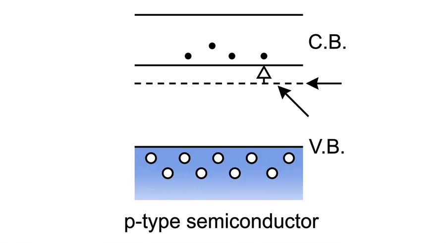
- With only three valence electrons, the impurity is one short of completing four covalent bonds with its neighbours. One bond is left incomplete.
- An electron from a neighbouring bond can jump into this vacancy with only a little energy (about to ), and complete the fourth bond. This leaves a hole in the valence band where the electron came from. The impurity atom, now having an extra electron, becomes a fixed negative ion (for example ). Because it accepts an electron from the valence band, it is called an acceptor.
- The acceptor atoms do not interact, so their states form a discrete acceptor level , just above the valence band.
- Accepting an electron creates a hole without creating a conduction electron. The hole can move freely through the valence band, but the negative ion is fixed in its place by its bonds.
How a p-type semiconductor behaves with temperature:
- At the acceptor levels are empty and the valence band is full. The conduction band is also empty. The material is an insulator.
- With a little heating (energy of the order of ), valence electrons jump into the acceptor levels, leaving holes in the valence band. At normal temperatures the acceptor levels are saturated (all filled), and a few electrons are also excited into the conduction band.
- At high temperatures, thermally generated electron-hole pairs dominate and far outnumber the holes produced by the acceptors.
Holes far outnumber electrons, so holes are the majority carriers and electrons are the minority carriers. Hence p-type (positive carriers).
Three temperature regimes
The temperature behaviour described above has three clear stages, shown here for n-type silicon with donors per .
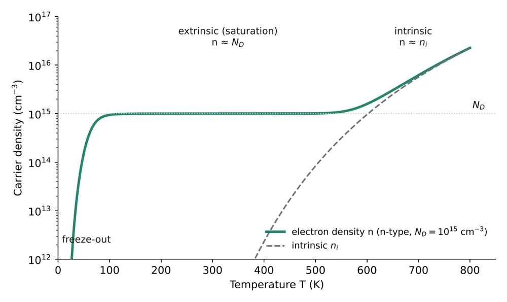
- Freeze-out (low temperature). There is too little thermal energy even to ionise the donors. Most donor electrons are "frozen" in , and increases rapidly as the temperature increases.
- Extrinsic or saturation region (roughly to for this doping). All donors are ionised, so , and is still far below . The carrier density is constant, independent of temperature. Devices are designed to work in this flat region, and this is why doping gives stable conductivity.
- Intrinsic region (high temperature). has grown until it is comparable to and then greater than . Electron-hole pairs across the gap now dominate, and the material behaves as intrinsic: , rising steeply with temperature. Doped devices stop working properly here, which is why silicon devices have a maximum operating temperature.
Heavier doping or a wider band gap pushes the intrinsic region to a higher temperature. This is one reason why silicon (gap ) replaced germanium (gap ) in most electronics: germanium becomes intrinsic at a much lower temperature.
Summary
| n-type | p-type | |
|---|---|---|
| Dopant | pentavalent (P, As, Sb) | trivalent (B, Ga, In) |
| Impurity called | donor | acceptor |
| Impurity level | , just below | , just above |
| Fixed ion left behind | positive | negative |
| Majority carriers | electrons | holes |
| Minority carriers | holes | electrons |
| Carrier density in the working range |
Watch out. An n-type semiconductor is not negatively charged, and a p-type is not positively charged. Each extra electron is balanced by a positive donor ion, and each hole by a negative acceptor ion, so the crystal as a whole is neutral. "n" and "p" tell the sign of the majority mobile carriers, not the net charge.
Page 9 of 18
Carrier densities in doped semiconductors
Beyond the syllabus. The syllabus treats extrinsic semiconductors qualitatively. This page shows, with two simple equations that you already have, how many majority and minority carriers a doped sample has. It makes the law of mass action, the Fermi level and the p-n junction much easier to understand.
Two equations
Take an n-type sample with donors per unit volume, all ionised (the extrinsic region of the previous page).
1. Charge neutrality. The sample as a whole is neutral. The positive charges are the holes and the donor ions. The negative charges are the electrons:
2. Law of mass action. At any temperature,
Majority and minority carriers
In the normal case . Then is tiny, the in the neutrality equation is negligible, and
For a p-type sample with acceptors per unit volume, in the same way,
- The majority carrier density is decided by the doping and hardly depends on temperature.
- The minority carrier density is decided by and so rises steeply with temperature. This is why the reverse current of a diode, which is carried by minority carriers, is so sensitive to temperature (page 15).
- Doping increases the majority carriers and decreases the minority carriers below the intrinsic value. Adding donors does not only add electrons. It also removes holes, because the extra electrons recombine with them.
Example. Silicon with is doped with donors. Then
The electrons outnumber the holes by a factor of about .
Where the Fermi level sits
Combining with gives the position of the Fermi level directly:
and similarly for p-type.
Example. For the silicon above at with :
The Fermi level is below the conduction band, well above mid-gap (which is about below ). Each tenfold increase in moves it up by .
Key idea. Doping does not change (a property of the pure material). It changes how the fixed product is shared between electrons and holes, and the Fermi level moves to whatever position gives that sharing.
Watch out. uses squared. If you forget the square, the answer will be wrong by a factor of .
Page 10 of 18
Fermi level in semiconductors
The Fermi level is the energy at which the occupation probability is . In a semiconductor no states exist there (it lies in the gap), but its position is still very important. By the results of pages 5 and 6, depends on how far is below , and on how far it is above . So we can read the carrier balance from the Fermi level.
Intrinsic semiconductor
In an intrinsic semiconductor . Put the two results:
Cancel the common factors and :
Collect the exponentials on one side. Dividing both sides by and adding the exponents, :
Take natural logarithms:
Solve for :
- At the second term vanishes: . The Fermi level is exactly in the middle of the band gap.
- At higher temperatures it shifts slightly: up if , down if . The physical reason: the band with the larger effective mass has more states (larger or ), so to keep the Fermi level must move a little away from that band.
- The shift is tiny. For silicon, with density-of-states masses and , at it is , against a gap of . So the Fermi level of an intrinsic semiconductor is usually taken to be at the middle of the gap.
n-type semiconductor
The donor level lies just below the conduction band edge .
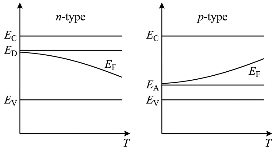
- At the donor level is full and the conduction band is empty, so the Fermi level (the boundary between filled and empty states) lies midway between and :
- Low temperatures. As the temperature rises, donor electrons move into the conduction band and the donor level starts to empty. The Fermi level moves down towards . When the donors are fully ionised (around the depletion temperature , so called because the donor level has been depleted of its electrons), it has fallen to about the donor level, .
- Extrinsic region. Now is fixed, but increases as and also increases, so by the Fermi level keeps falling, roughly linearly with .
- High temperatures. Once intrinsic carriers dominate, the material behaves as intrinsic. Above the intrinsic temperature the Fermi level reaches the middle of the gap: .
p-type semiconductor
The acceptor level lies just above the valence band edge .
- At the acceptor level is empty and the valence band is full, so the Fermi level lies midway between and :
- Low temperatures. Holes in the valence band come only from the acceptors. As valence electrons fill the acceptor levels, the Fermi level moves up towards . When the acceptors are saturated (around the saturation temperature ), it reaches about the acceptor level, .
- Extrinsic region. With fixed, increases with , so the Fermi level keeps rising, roughly linearly.
- High temperatures. Above the material is intrinsic and , at mid-gap.
Effect of doping level
At a fixed temperature in the extrinsic region:
- more donors push the Fermi level closer to the conduction band ( becomes smaller);
- more acceptors push it closer to the valence band.
If the doping is so heavy that the Fermi level reaches the band edge or enters the band, the semiconductor is called degenerate, and the Boltzmann approximation (and so all the formulas above) is no longer valid. Tunnel diodes (Module 4) use such degenerate doping.
Key idea. Doping pushes the Fermi level towards the band with the majority carriers: up for n-type, down for p-type. Heating always pulls it back towards the middle of the gap, because at high temperature every semiconductor becomes intrinsic.
Watch out. In the intrinsic derivation, the masses appear as , with holes on top. If you write the ratio upside down, the direction of the shift is reversed. Also remember that belongs to n-type (donors depleted) and to p-type (acceptors saturated).
Page 11 of 18
Conductivity of semiconductors
Beyond the syllabus. Module 1 gave for a metal. In a semiconductor, both electrons and holes carry current, and this short page shows how to combine them. It explains in numbers why doping is so important.
Two kinds of carrier
In an electric field , electrons drift against the field and holes drift with it. Because their charges are opposite, both produce current in the same direction, so the two contributions add:
where and are the electron and hole mobilities. Comparing with :
- Intrinsic: , so .
- n-type: , so .
- p-type: , so .
Electrons usually have a higher mobility than holes (in silicon and ), because their effective mass for conduction is smaller.
Worked examples
Intrinsic silicon at room temperature, :
Intrinsic germanium, , , :
about five thousand times better than silicon, because of its smaller gap.
Doped silicon with ():
That is about half a million times the intrinsic value, from one dopant atom for five million silicon atoms. Its resistivity is .
Temperature dependence
- Intrinsic: follows , so it rises steeply (exponentially) with temperature. The mobilities fall slowly as lattice vibrations increase, but this is completely overcome by the rise in . Hence the negative temperature coefficient of resistance of semiconductors.
- Extrinsic region: is constant, so changes only through the mobility, which falls slightly with temperature. Over this range a doped semiconductor behaves rather like a metal, with a small positive temperature coefficient.
Watch out. In the two terms add, even though electrons and holes move in opposite directions. Opposite charge and opposite velocity give current in the same direction.
Page 12 of 18
Forming a p-n junction
Why junctions matter
On its own, a p-type or n-type crystal just conducts like a poor conductor, with the same resistance whichever way the current flows. It has no important use as such. Nearly all semiconductor devices combine the two types. The simplest is a single p-n junction, or p-n junction diode: one crystal that is p-type on one side and n-type on the other, made by special manufacturing processes (diffusing or growing dopants into a single crystal). Simply pressing two pieces together does not work, because the surfaces would not make a perfect crystal contact.
Diffusion and the depletion region
The p-side has many holes and few electrons. The n-side has many electrons and few holes. At the moment the junction is formed:
- Diffusion. Any particles that are more concentrated in one place than another spread out, just as ink spreads in water. So electrons diffuse from n to p and holes diffuse from p to n. This movement caused by a difference in concentration is called diffusion, and the current it carries is the diffusion current.
- Recombination. Near the junction, the diffusing electrons and holes meet and recombine: conduction electrons fall into holes and become bound valence electrons. Both carriers disappear.
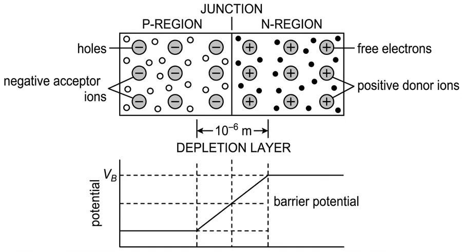
- A region without mobile carriers. A thin region on both sides of the junction is left without mobile carriers. This is the depletion region (depleted of carriers). It is about wide, narrower for heavier doping, and because it has no free carriers, it behaves like an insulator.
- Uncovered ions. What is left in the depletion region are the fixed ions. On the p-side, each acceptor that has lost its hole is now an uncovered negative ion. On the n-side, each donor that has lost its electron is an uncovered positive ion. These ions cannot move, so the depletion region has a net charge on each side and is also called the space charge region. The total charge on the two sides is equal and opposite.
Barrier potential
The double layer of ions (positive on the n-side, negative on the p-side) produces an electric field inside the depletion region, pointing from the positive donor ions (n-side) to the negative acceptor ions (p-side).
This field acts on any carrier that wanders into the region:
- it pushes electrons back towards the n-side, and
- it pushes holes back towards the p-side.
So it opposes further diffusion of the majority carriers. As more carriers diffuse and recombine, the ion layers grow, the field becomes stronger, and diffusion is resisted more and more. The process is self-limiting.
The potential difference across the depletion region is the barrier potential (junction potential or built-in potential) : about for silicon and for germanium. A majority electron on the n-side needs an energy to climb over this barrier.
Beyond the syllabus. By combining the results of pages 5, 6 and 9, we get the built-in potential as . For silicon with and at this is , in agreement with the quoted for silicon.
Drift of minority carriers
There are also a few minority carriers on each side: holes in the n-region and electrons in the p-region, created by thermal generation. If one of them reaches the edge of the depletion region, the junction field does not stop it. It sweeps it across. A hole from the n-side is pushed to the p-side, and an electron from the p-side is pushed to the n-side.
Movement caused by an electric field is called drift, and this flow is the drift current. It is small, because minority carriers are few, and it does not depend on the height of the barrier: every minority carrier that arrives at the edge is swept across, however strong the field. So it reaches a saturation value decided by the rate at which minority carriers are generated, which depends on temperature.
Key idea. At equilibrium, the diffusion current of majority carriers is exactly balanced by the drift current of minority carriers in the opposite direction, so the net current is zero. Both currents still flow, but they cancel each other.
Band diagram of the junction
Before contact, the n-side bands sit lower in energy than the p-side bands, because the Fermi level of n-type is near its conduction band and that of p-type is near its valence band. When high-energy electrons cross from n to p, the n-side loses negative charge and becomes positive, which lowers the electron energy there. So the n-side bands move down relative to the p-side. Equilibrium is reached when the Fermi levels on the two sides are equal.
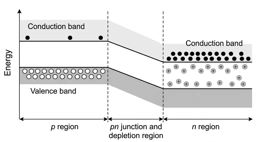
- The bands now bend across the depletion region. An electron in the n-side conduction band has to climb an energy hill of height to reach the p-side. A hole on the p-side faces the same hill, upside down, to reach the n-side (for holes, energy increases downwards on the diagram).
- Both the conduction band and the valence band shift by the same amount, so the band gap is unchanged on each side: it still takes the same energy for a valence electron to become a free electron.
Why the Fermi levels must line up
Before contact, the Fermi level of the n-type material is near its conduction band and that of the p-type is near its valence band. The Fermi level behaves like a "level" of electron energy, in the same way that water finds a common level in connected tanks or heat flows until temperatures are equal. In a system in thermal equilibrium it must be the same everywhere. If it were higher on one side, electrons there would have more states occupied at a given energy than on the other side and would flow across until the difference disappears. So electrons flow from the side with the higher Fermi level (n) to the side with the lower one (p) until the two match, and the band edges in the two regions shift to make this alignment possible.
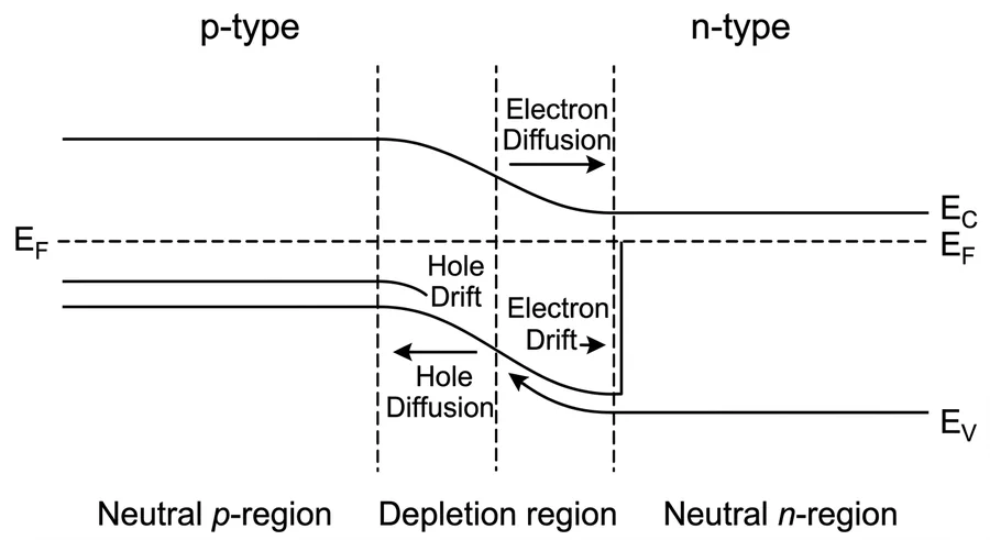
Note on the source. The lecture notes described the electron flow as continuing "until the top of the conduction band of the n-region aligns with the bottom of the conduction band of the p-region". The correct condition is that the Fermi levels align. The conduction band edges then differ by , as the band diagram shows.
Watch out. The junction field points from n to p, because the n-side is left with positive ions. It pushes electrons back towards n and holes back towards p, and this is what stops the diffusion. Do not draw the depletion region as charged on one side only: both sides have equal and opposite charge.
Page 13 of 18
Biasing a p-n junction
Applying an external voltage across the junction is called biasing. The external battery adds its own electric field to the built-in field of the junction. Which way the battery is connected decides whether the two fields add or oppose, and that decides almost everything.
Forward bias
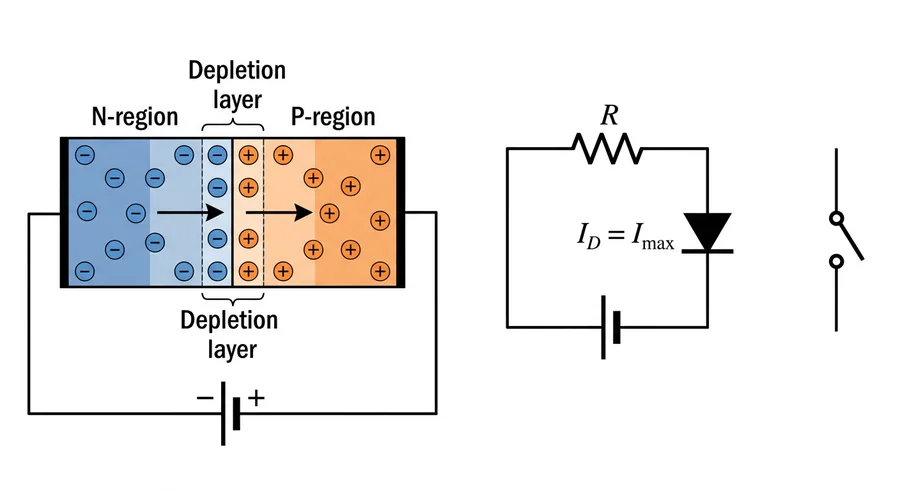
Forward bias. The p-side is connected to the positive terminal and the n-side to the negative terminal.
What happens, step by step:
- The applied field points from p to n through the junction, opposite to the built-in field (which points from n to p). So the net field across the junction is smaller than the built-in field.
- The positive terminal pushes the holes in the p-region towards the junction, and the negative terminal pushes the electrons in the n-region towards it. They neutralise some of the fixed ions at the edges of the depletion region, so the depletion region becomes narrow and less resistive.
- The barrier height falls from to . The number of majority carriers that can climb a barrier depends exponentially on its height, so even a small reduction lets many more carriers go over. The diffusion current increases enormously.
- At about for germanium and for silicon, the barrier is effectively removed and the depletion region offers negligible resistance. Majority carriers then cross easily and the current rises steeply.
- The drift current of minority carriers does not change (it never depended on the barrier height), so it is now very small compared with the much larger diffusion current.
What happens in the external circuit:
- A free electron that crosses from n to p recombines with a hole in the p-region and becomes a valence electron. It continues through the p-region by hopping from hole to hole (as valence-band current) to the positive terminal.
- To replace it, the negative terminal injects another electron into the n-region.
- At the same time, the positive terminal pulls an electron out of a covalent bond in the p-region, creating a new hole there. The electron enters the external circuit. The hole stays in the p-region and moves towards the junction.
- The result is a large, steady current: through the diode it is carried by majority carriers, and in the wires it is carried by electrons.
Reverse bias
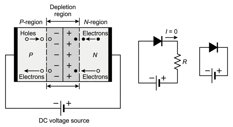
Reverse bias. The p-side is connected to the negative terminal and the n-side to the positive terminal.
What happens:
- The applied field is in the same direction as the built-in field, so the net field across the junction is larger.
- The negative terminal pulls the holes away from the junction on the p-side, and the positive terminal pulls the electrons away on the n-side. More fixed ions are uncovered, so the depletion region becomes wider and more resistive.
- The barrier height rises to . Hardly any majority carriers can climb it, so the diffusion current falls almost to zero.
- Minority carriers are still swept across by the (now stronger) field, giving a small reverse current. Their number is fixed by temperature, not by voltage, so once the reverse voltage is more than a few tenths of a volt, the reverse current saturates at a constant value, the reverse saturation current .
- A very large reverse voltage causes breakdown of the junction (page 15).
Comparison
| Forward bias | Reverse bias | |
|---|---|---|
| Connection | p to , n to | p to , n to |
| Applied field vs built-in field | opposite | same direction |
| Depletion region | narrower | wider |
| Barrier height | lowered, to | raised, to |
| Main current | diffusion of majority carriers | drift of minority carriers |
| Size of current | large (mA to A), rises exponentially | tiny ( or nA), saturates |
| Diode acts as | a closed switch (low resistance) | an open switch (high resistance) |
This one-way behaviour, conducting in one direction and blocking in the other, is what makes the diode useful. It is the basis of the rectifiers in Module 4.
Watch out. "Forward" means p to positive. A common mistake is to remember it the other way round. Think "positive to p". Also, in reverse bias the depletion region becomes wider, not narrower.
Page 14 of 18
The diode equation
The idea
The diode equation gives the current through a p-n junction as a function of the applied voltage . It changes the qualitative picture of the last page into a formula. The total current is the sum of an electron current and a hole current:
We derive in detail. follows in exactly the same way.
At equilibrium (no bias), electrons diffuse from n to p (majority carriers) and electrons drift from p to n (minority carriers pulled by the barrier field), and the two currents are equal. The same is true for holes. The key question is: how does the applied voltage disturb this balance?
Step 1: electron density on each side at equilibrium
We use the result of page 5, , on each side of the junction. The Fermi level is the same on both sides (page 12), and this lets us compare them.
Take the top of the n-side valence band as the zero of energy. Then the bottom of the n-side conduction band is at , and
On the p-side the bands are raised by the barrier energy , so the bottom of its conduction band is at . (The gap on the p-side is still . The extra is the band bending due to the formation of the junction.) Its electron density is
On dividing, , and all cancel:
Meaning. The minority electron density on the p-side is equal to the majority density on the n-side multiplied by the Boltzmann factor for climbing the barrier. Only those n-side electrons that have enough energy to climb are found on the p-side. For silicon, with at , the factor is about .
At equilibrium, diffusion and drift balance and this density stays fixed.
Step 2: apply a forward voltage
The barrier falls from to . Two things happen:
- Diffusion increases. More n-side electrons now have enough energy to climb the lower barrier, so more of them reach the p-side.
- Drift stays almost the same. The drift current is decided by how many minority electrons are generated on the p-side, which depends on temperature, not on the barrier.
The new electron density on the p-side, just at the edge of the junction, is given by the same Boltzmann relation with the lower barrier:
So the applied voltage multiplies the electron density on the p-side by . This exponential factor is the heart of the diode equation.
Step 3: the extra electrons give the current
The increase in the electron density on the p-side is
These extra (injected) electrons diffuse into the p-region and recombine there, and as they do so, new electrons must keep crossing the junction to replace them. The resulting electron current is proportional to this excess:
where is a constant (it contains and the factors describing diffusion). The is the drift current, which still flows the other way and is subtracted.
In exactly the same way, holes injected from the p-side into the n-side give a hole current
Step 4: add
This is the diode equation.
Special cases
- Reverse bias, :
For a reverse voltage of more than a few tenths of a volt, and . The minus sign means the current flows the other way, from n to p. This is the largest reverse current at that temperature (before breakdown), so is called the reverse saturation current. Physically it is just the drift current of minority carriers, with no diffusion to cancel it.
- Large forward bias, : the is negligible and
The current becomes ten times for every increase in of at room temperature.
-
No bias, : . No current flows without an applied voltage, because diffusion and drift balance exactly.
-
Practical diodes differ a little from the ideal equation (for example, because some carriers recombine inside the depletion region). This is taken care of by an ideality factor :
is taken as about for germanium and for silicon, so it is also called the material constant.
- Thermal voltage. The combination (about at ) is the thermal voltage, and the equation is often written
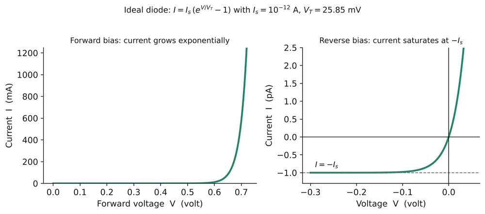
Temperature and the saturation current
is carried by minority carriers, whose density is or (page 9). So , which rises extremely fast with temperature. In practice the reverse saturation current of a silicon diode roughly doubles for every rise. This is why diode circuits are temperature sensitive.
Watch out. In use consistent units: either in coulombs with in J/K, or (simpler) write with in eV, so that is just volts. Also keep the . It makes the current zero at and equal to in reverse bias.
Page 15 of 18
V-I characteristics of a p-n junction
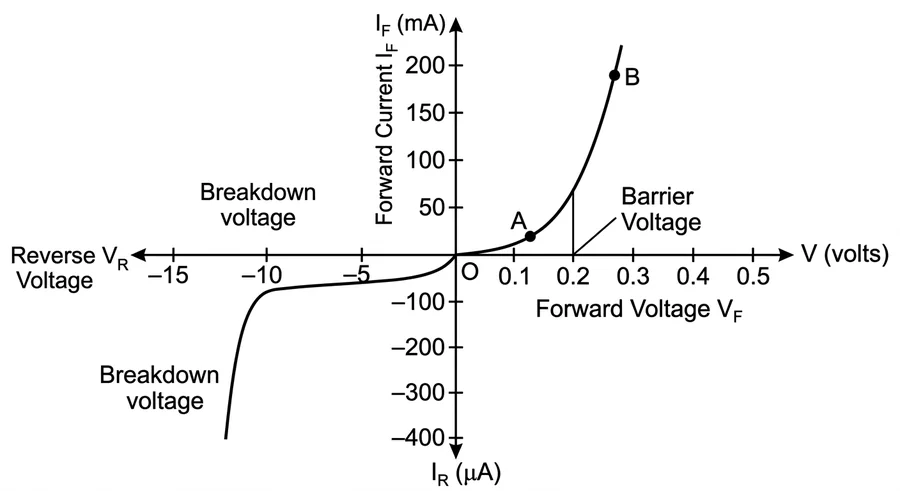
A V-I characteristic (volt-ampere characteristic) is a graph of the current through a device against the voltage across it. For a p-n junction diode it has three regions.
How the graph is measured
The diode is connected in series with a resistor (to limit the current) and a variable supply, with a voltmeter across the diode and a milliammeter (forward) or microammeter (reverse) in series. The supply is increased in small steps and the current is noted at each voltage, first in forward bias and then, with the supply reversed, in reverse bias.
1. Forward bias region
- While the forward voltage is less than the barrier potential , the barrier still blocks most majority carriers and the current is very small (region OA in the figure).
- When reaches about , the current starts to rise sharply. This voltage is the knee voltage (cut-in voltage or threshold voltage): about for germanium and for silicon. It is where the curve "bends like a knee".
- Beyond it, the barrier has effectively gone and the forward current rises exponentially, as the diode equation predicts (region AB). In a real diode the rise finally becomes more nearly straight, because the resistance of the bulk p and n regions starts to limit the current.
- The knee is not a sharp physical threshold. The current is exponential everywhere. It looks like a knee only because, on a linear milliampere scale, the current cannot be seen until it reaches a noticeable size.
2. Reverse bias region
- Practically no current flows. Only the minority carriers cross, giving a tiny reverse current, carried by drift.
- The number of minority carriers is fixed by the temperature, not by the voltage, so the reverse current quickly reaches a constant value, the reverse saturation current , and stays there as the reverse voltage increases.
- The reverse current is so much smaller than the forward current (microamperes or nanoamperes against milliamperes) that it is drawn on a different scale.
- Because , the reverse current rises steeply with temperature.
3. Breakdown region
- When the reverse voltage is increased enough, the field in the depletion region becomes very strong. The minority carriers crossing it gain so much kinetic energy that they knock electrons out of the covalent bonds of the semiconductor atoms (ionisation by collision). Each freed electron is accelerated in turn and frees more electrons, a chain reaction called an avalanche.
- The reverse current rises suddenly and the junction resistance falls. The reverse voltage at which this happens is the breakdown voltage.
- In an ordinary diode, the large current and power at breakdown heat the junction and can permanently damage it, so an ordinary diode is never operated in this region.
- In very heavily doped junctions, breakdown happens instead by Zener breakdown, in which the strong field pulls electrons directly out of their bonds (by tunnelling). Zener diodes, in Module 4, are designed to work safely in breakdown.
Static and dynamic resistance
Two useful ways of describing the curve:
- Static (DC) resistance at a point: .
- Dynamic (AC) resistance: the reciprocal of the slope, . From the diode equation, for forward bias : at and room temperature with , . It is small in forward bias and very large in reverse bias.
Watch out. The two halves of the graph use different current scales: milliamperes forward, microamperes reverse. Label both axes when you draw it, and mark the knee voltage and the breakdown voltage.
Page 16 of 18
Numerical problems
Constants used: . In the diode problems is calculated as .
Intrinsic carriers and band gap
Problem 1. The forbidden gap of pure silicon is . Compare the number of conduction electrons at and .
From , with and :
A rise roughly doubles the number of conduction electrons. Notice that almost all of this comes from the exponential; the factor contributes only 5 %.
Problem 2. An intrinsic semiconductor has and effective density of states . Find the electron density at , using .
Note on the source. The lecture notes rounded the exponent to and got . If we keep more digits, we get . Exponentials are sensitive, so round only at the end.
About the formula. is the exact result with the assumption . The next two problems use the same assumption.
Problem 3. For silicon at , and . Find the band gap.
Rearranging : divide by , take logarithms and multiply by , to get :
Problem 4. At an intrinsic semiconductor has and electron density . Find its band gap.
Diode current
In problems 5 to 10 take unless stated.
Problem 5. A p-n junction carries at room temperature () under a large reverse bias. Find the current for a forward bias of .
The current under large reverse bias is the saturation current, . With :
Problem 6. A silicon diode at has reverse saturation current . Find the current for a forward bias of .
Problem 7. In a rectifier circuit at the forward current is at . Find the reverse saturation current.
With , :
Problem 8. A diode has . Find the forward voltage for , using .
Rearranging : , so
Problem 9. A silicon diode has and . Find the current at .
Problem 10. A diode has , and ideality factor . Find the current at .
About problems 6 and 9. Answers of a few amperes come directly from the ideal diode equation. A real small diode would never pass that much current at or , because its series resistance and the external circuit limit the current. Treat these as exercises in using the formula, not as realistic currents.
Watch out. Check what the question gives: "room temperature" means take or (say which one). A current under "large reverse bias" is . And given in millivolts must be changed to volts before dividing.
Page 17 of 18
More worked examples
These go a little beyond the standard problems, to practise the ideas on pages 3 to 15. Constants: , , , .
Example 1. Size of . Find the effective density of states in the conduction band at for an electron effective mass equal to the free-electron mass.
The bracket is , so . For a different effective mass, multiply by . With (silicon) this gives , the value used in the problems.
Example 2. Is the Boltzmann approximation good? In intrinsic silicon the Fermi level is about below . Compare the exact Fermi-Dirac occupation at the band edge with the Boltzmann value at .
.
They agree to better than one part in a billion. The approximation is essentially exact here.
Example 3. Heating silicon by . By what factor does of silicon () increase from to ?
A modest rise in temperature multiplies the intrinsic carriers almost thirty times.
Example 4. Germanium against silicon. Assuming equal and , estimate how many times more intrinsic carriers germanium () has than silicon () at .
The quoted values ( and ) give a ratio of about . The difference comes from the different , of the two materials. In both cases the difference in the gap is the deciding factor.
Example 5. Minority carriers in p-type silicon. Silicon at (, ) is doped with acceptors. Find , and the position of the Fermi level.
The Fermi level is only above the valence band, far below mid-gap.
Example 6. Effect of doping on conductivity. By what factor does doping silicon with increase its conductivity? Take , , .
Example 7. Barrier and minority electrons. In a silicon junction with at , what fraction of the n-side electron density is found on the p-side at equilibrium?
Example 8. Voltage for a tenfold current. For an ideal diode () at in forward bias, how much must the voltage increase to make the current ten times?
With , a tenfold increase needs , so
This "60 mV per decade" rule is why the forward voltage of a silicon diode stays close to to over a huge range of currents.
Example 9. Forward against reverse. For a diode at , how many times larger is the forward current at than the magnitude of the reverse current?
Even at a tenth of a volt, the diode already conducts nearly fifty times better in the forward direction than in the reverse direction. At the ratio is about .
Page 18 of 18
Practice questions and formula sheet
Short questions to revise
- What is a hole? Why does it behave like a positive charge, and why does it move opposite to the electrons?
- What is effective mass? Why is the effective mass of a valence-band electron near the band top negative, and why do we use holes instead?
- Write the density of states formula and explain each symbol. Why is there a factor ?
- Derive the expression for the density of electrons in the conduction band of an intrinsic semiconductor. Justify the Boltzmann approximation.
- Derive the expression for the density of holes in the valence band.
- Derive the intrinsic carrier concentration. State and explain the law of mass action.
- How does vary with temperature and with band gap? Why does not depend on the Fermi level?
- Distinguish between n-type and p-type semiconductors, with band diagrams.
- Describe the freeze-out, extrinsic and intrinsic regions of a doped semiconductor.
- Show that the Fermi level of an intrinsic semiconductor lies at the middle of the gap at .
- How does the Fermi level of an n-type semiconductor change with temperature? Of a p-type?
- Explain the formation of a p-n junction and the depletion region in terms of diffusion and drift. Draw its energy band diagram.
- Why must the Fermi levels on the two sides of a junction be equal at equilibrium?
- What happens to the depletion region, the barrier and the currents under forward and reverse bias?
- Derive the diode equation. What is the reverse saturation current, and why does it saturate?
- Draw and explain the V-I characteristic of a p-n junction diode. What is the knee voltage? What causes breakdown?
Quick numerical practice
- The band gap of germanium is . By what factor does change between and ? (Answer: about , from .)
- A diode has at . Find the current for a forward bias of (). (Answer: .)
- Silicon () is doped with . Find the hole density. (Answer: .)
- Find the dynamic resistance of an ideal diode carrying at . (Answer: .)
Formula sheet
Carrier densities
| Density of states | |
| Standard integral | |
| Boltzmann approximation | (electrons), (holes) |
| Electrons | , |
| Holes | , |
| Intrinsic concentration | |
| Law of mass action | |
| Temperature dependence | |
| Doped (beyond syllabus) | n-type: , ; p-type: , |
| Conductivity (beyond syllabus) |
Fermi level
| Intrinsic | , mid-gap at |
| n-type at | , moves down towards mid-gap as rises |
| p-type at | , moves up towards mid-gap as rises |
| Doped, extrinsic region (beyond syllabus) | , |
The p-n junction
| Barrier potential | about (Si), (Ge); (beyond syllabus) |
| Electron densities | |
| Diode equation | |
| Thermal voltage | at |
| Reverse bias | |
| Large forward bias | ; about 60 mV per tenfold current at () |
| Dynamic resistance | |
| Ideality factor | (Ge), (Si) |