
Page 1 of 15
Module 4 at a glance
Module 3 explained what happens inside a p-n junction: how it forms, how it behaves in forward and reverse bias, and the diode equation. This module uses junctions as devices. Almost every electronic gadget you use has several of them.
- Rectifiers change the AC from the mains into DC, using ordinary diodes as one-way valves.
- Special diodes use the junction in special ways: the Zener diode works deliberately in breakdown to keep a voltage steady, and the tunnel diode uses quantum tunnelling (Module 2) to give a negative resistance.
- Photonic devices connect electricity and light: the LED changes current into light, photodiodes and solar cells change light into current, and the semiconductor laser produces a coherent beam.
KTU syllabus. Semiconductor devices: rectifiers, full wave and half wave. Zener diode, V-I characteristics. Tunnel diode, V-I characteristics. Semiconductor laser (construction and working), applications. Photonic devices (qualitative treatment only): photodetectors (junction and PIN photodiodes), solar cells (I-V characteristics, efficiency, stringing of solar cells to a solar panel), light emitting diode, applications.
What you will be able to do
- Explain the working of half-wave, centre-tap full-wave and bridge rectifiers in each half cycle, with circuit diagrams and waveforms.
- Derive , , , efficiency, ripple factor and form factor, and write the peak inverse voltage of each rectifier.
- Compare the three rectifiers and explain why a filter is used.
- Explain avalanche and Zener breakdown physically, and design a simple Zener voltage regulator.
- Explain the tunnel diode with band diagrams at each part of its V-I curve, including the negative resistance region.
- Explain how an LED produces light and how its colour depends on the band gap.
- Explain the p-n and PIN photodiodes and compare them.
- Explain how a solar cell works, read its I-V curve, and calculate efficiency and fill factor. Build a module and an array from cells.
- Describe the construction and working of a semiconductor laser, and compare it with an LED.
How to use these notes
- Each page follows the same shape: idea → working or derivation → key results → worked example → common mistakes.
- Green boxes show key ideas. Amber boxes marked Watch out show mistakes that make you lose marks. Boxes marked Note on the source show where the lecture notes were corrected.
- A few short sections are marked beyond the syllabus. They are given because they make the syllabus topics easier to understand. You will not be asked about them directly in the exam.
- The numerical problems from the lecture notes are worked in full on their own page. The last page has practice questions with answers and a formula sheet.
Where each topic sits
| Part | Pages |
|---|---|
| Rectifiers | Rectifier basics, half-wave, centre-tap full-wave, bridge, comparison and filters |
| Special diodes | Breakdown, Zener diode and regulator, tunnel diode |
| Photonic devices | LED, photodetectors, solar cells, semiconductor laser |
| Problems | Numerical problems, practice and formula sheet |
Before you start. You should know Module 3: the p-n junction, forward and reverse bias, the depletion region, the diode V-I characteristic and energy band diagrams. From Module 2: tunnelling. For the rectifier derivations you need , the identity , and .
Page 2 of 15
Rectifiers: the basic ideas
Why we need rectifiers
The mains supply is alternating current (AC): in India it is rms at . Its voltage changes direction 100 times every second. Electronic circuits (phones, computers, amplifiers) need direct current (DC): a voltage of one fixed polarity, usually only a few volts.
Rectifier. A rectifier is an electronic circuit that changes an AC input voltage into a DC output voltage.
A rectifier works because a p-n junction diode is a one-way device: it conducts when forward biased and blocks current when reverse biased. Placed in the path of an alternating current, it lets through only the half cycles in which it is forward biased.
The DC power supply
A complete DC power supply has four stages:
| Stage | What it does |
|---|---|
| Transformer | steps the mains voltage down (or up) to the level needed, and isolates the circuit from the mains |
| Rectifier | converts the AC into pulsating DC (this page and the next three) |
| Filter | smooths out the pulsations (ripple), usually with a capacitor |
| Regulator | holds the output voltage constant, for example with a Zener diode |
Symbols used
| Symbol | Meaning |
|---|---|
| instantaneous voltage applied to the rectifier (the transformer secondary) | |
| peak (maximum) value of that voltage; | |
| forward resistance of a conducting diode | |
| load resistance | |
| peak current, | |
| period of the AC, ; , so |
Quantities that describe a rectifier
Average (DC) value. The output is not a steady DC, but it has an average value over one cycle. A DC meter reads this average. For a current,
RMS value. The root mean square value is the square root of the mean of the squares of the instantaneous values. It shows the heating (power) effect of the whole waveform, both its DC and its AC parts:
Rectifier efficiency. How much of the AC power given to the rectifier comes out as useful DC power in the load:
The DC output power is that of the average current in the load, . The AC input power is everything delivered to the circuit, , including the power lost as heat in the diode.
Ripple factor. The rectified output has the wanted DC plus unwanted AC components, called ripple. The ripple factor compares the two:
Because (the DC and AC parts add in power),
The smaller the ripple factor, the closer the output is to pure DC, and the better the rectifier.
Form factor and peak factor. Two shape ratios that are often asked:
Notice that .
Peak inverse voltage (PIV). The maximum reverse voltage that appears across a diode during the half cycle in which it does not conduct. The diode must be chosen with a reverse voltage rating above the PIV, or it will break down.
Key idea. Every rectifier result follows from just two integrals, and . Learn to derive these two, and then efficiency, ripple factor and form factor follow in one line each.
Watch out. Efficiency uses in the denominator but only in the numerator. The power wasted as heat in the diode is part of the input but not of the useful output.
Page 3 of 15
The half-wave rectifier
Circuit
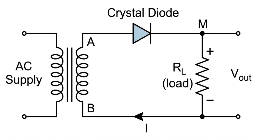
The half-wave rectifier is the simplest rectifier: a transformer, one diode, and the load resistor in series.
Working
When the AC supply is switched on, the alternating voltage appears across the terminals A and B of the transformer secondary.
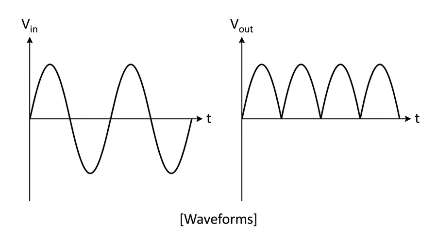
- Positive half cycle. End A is positive and end B is negative. The diode is forward biased and conducts. Current flows from A through the diode, through (from M towards B), and back to B. The voltage across follows the input.
- Negative half cycle. End A is negative and end B is positive. The diode is reverse biased and does not conduct. No current flows, and the output is zero. The whole secondary voltage now appears across the diode in reverse.
The current through always flows in the same direction, so it is DC. But its magnitude is not constant. It is a series of positive half-sine pulses with gaps between them, called pulsating DC.
Average (DC) current
Let the input be . In the positive half cycle the circuit resistance is , so the current is
Average over one full cycle:
The DC output voltage is
which is when .
RMS current
Efficiency
The efficiency is largest when : the maximum efficiency is 40.6 %. (Exactly, , so 40.5 %, but most books quote 40.6 %.) Less than half of the AC input power appears as DC power in the load. The rest is in the ripple, and heat in the diode.
Ripple factor, form factor and peak factor
A ripple factor above 1 means the AC part of the output is larger than the DC part: a very poor DC.
Peak inverse voltage
PIV of a half-wave rectifier. During the negative half cycle the diode does not conduct, so no current flows in and there is no voltage across it. The whole secondary voltage appears across the diode in reverse. Its maximum is the peak secondary voltage: .
Advantages and disadvantages
| Advantages | Disadvantages |
|---|---|
| only one diode | low efficiency (at most 40.6 %) |
| simple and cheap | high ripple factor (1.21): needs heavy filtering |
| no centre tap on the transformer | output current is intermittent: nothing flows for half of each cycle |
| the transformer carries a DC component, which can saturate its core |
Worked example
Example. A half-wave rectifier is fed from the , mains through a step-down transformer. The load is and the diode resistance is negligible. Find , , , , the rms ripple voltage and the PIV.
The secondary rms voltage is , so
The rms ripple voltage is , larger than the DC itself. The diode must withstand .
Note on the source. The lecture notes described the half-wave PIV as the voltage "across the centre tap and one end", which belongs to the centre-tap full-wave circuit. For a half-wave rectifier the PIV is simply , the peak of the whole secondary voltage.
Watch out. and for half-wave. Do not mix them up with the full-wave values ( and ) on the next page. Also remember to change rms to peak first: a "23 V transformer" means , so .
Page 4 of 15
The full-wave rectifier with a centre-tapped transformer
The idea
A half-wave rectifier throws away every negative half cycle. A full-wave rectifier uses both half cycles: it turns the negative ones round so that they also drive current through the load in the same direction.
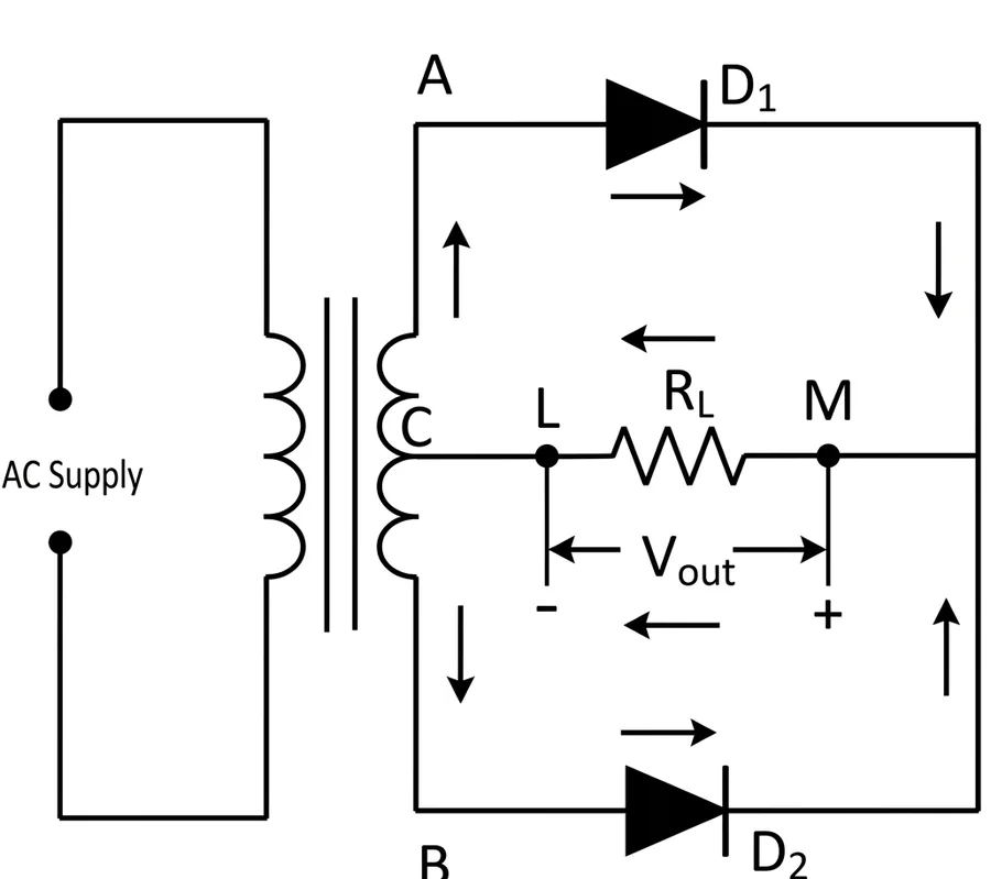
The centre-tap version uses a transformer whose secondary has a connection in the middle, the centre tap C, and two diodes. Each diode is fed by one half of the secondary. The load is connected between the joined cathodes (M) and the centre tap.
Working
When the supply is switched on, the alternating voltage appears across the secondary AB. Relative to the centre tap, ends A and B are always at opposite polarity.
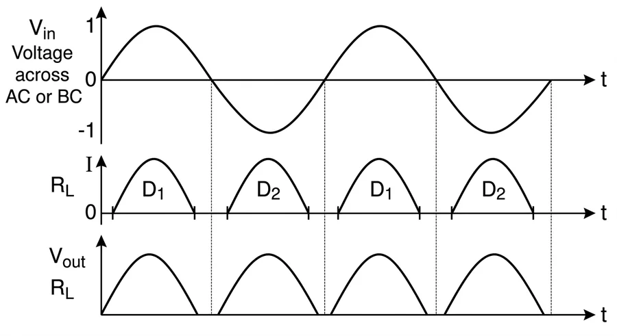
- Positive half cycle. End A is positive and end B is negative (relative to C). D1 is forward biased and conducts. D2 is reverse biased and does not conduct. Current flows from A, through D1, through from M to L, and back to the centre tap through the upper half of the secondary.
- Negative half cycle. End B is positive and end A is negative. D2 is forward biased and conducts. D1 does not conduct. Current flows from B, through D2, through again from M to L, and back through the lower half of the secondary.
The current through has the same direction in both half cycles, so the output is DC with a hump in every half cycle, not every other one. The output is still pulsating, but the gaps are gone.
Average current
Let the voltage from the centre tap to either end be . Each diode conducts for one half cycle with peak current , and both pulses go in the same direction through the load. So the current through is
The total over one cycle is twice the half-cycle value:
This is twice the half-wave value, as expected: there are twice as many pulses per cycle.
RMS current
is the same in both half cycles, so
(the integral was worked on the half-wave page).
This is the same as the rms value of a full sine wave, which makes sense: squaring removes the sign, so for a full-wave rectified sine is the same as for the original sine.
Efficiency
Only one diode conducts at a time, so the resistance in the current path is :
When , the maximum efficiency is 81.2 %, twice the half-wave value. (Exactly, , so 81.1 %, but most books quote 81.2 %.)
Ripple factor, form factor and peak factor
The ripple is still present, but it is less than half of the half-wave value, and its main frequency is ( for mains), which is easier to filter.
Peak inverse voltage
PIV of a centre-tap rectifier. Take the moment of the positive peak, when D1 conducts. The cathode of D2 is at the output voltage, about (ignoring the drop in D1), while its anode at end B is at . So D2 has across it in reverse: the whole secondary. Hence , where is the peak voltage of each half of the secondary.
Advantages and disadvantages
Advantages over the half-wave rectifier
- Higher efficiency: up to 81.2 %.
- Lower ripple factor: 0.48 instead of 1.21.
- Output current flows in both half cycles: it is continuous, though pulsating.
- The ripple frequency is , so a smaller filter does the job.
- The DC currents in the two halves of the secondary flow in opposite directions, so the transformer core is not magnetised by DC.
Disadvantages
- Two diodes are needed, and a transformer with a centre tap, which is more difficult to make.
- Each diode must withstand a PIV of .
- Each half of the secondary is used only half the time, so for a given output voltage the transformer must be larger.
Worked example
Example. A centre-tap full-wave rectifier uses a (rms) transformer, diodes with , and a load of . Find , , , the DC output power, the efficiency and the PIV.
Check with the formula: . The PIV is .
Watch out. In the centre-tap circuit is measured from the centre tap to one end, and each diode sees in reverse. Writing PIV here is a common mistake. Also, a "12-0-12 V" transformer gives rms on each half, so , not .
Page 5 of 15
The bridge rectifier
The idea
The bridge rectifier gives full-wave output without a centre tap, using four diodes arranged in a bridge (a diamond). The whole secondary winding is used in both half cycles.
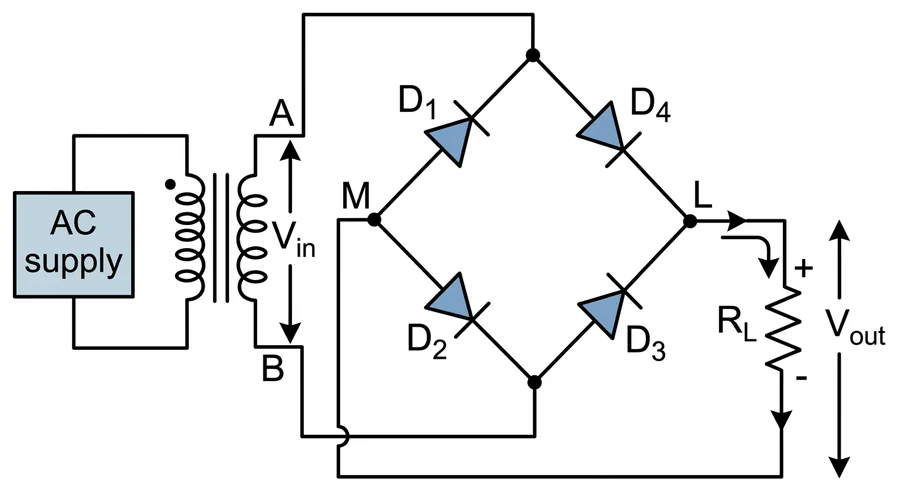
The AC input is applied across one diagonal of the bridge (A and B). The load is connected across the other diagonal (M and L).
Working
- Positive half cycle. End A is positive and end B is negative. Diodes D1 and D3 are forward biased and conduct. D2 and D4 are reverse biased and do not conduct. Current flows from A through D1, through from M to L, through D3 and back to B.
- Negative half cycle. End A is negative and end B is positive. Diodes D2 and D4 are forward biased and conduct. D1 and D3 do not conduct. Current flows from B through D2, through again from M to L, through D4 and back to A.
The load current has the same direction (M to L) in both half cycles, so a full-wave DC output is obtained across the load.
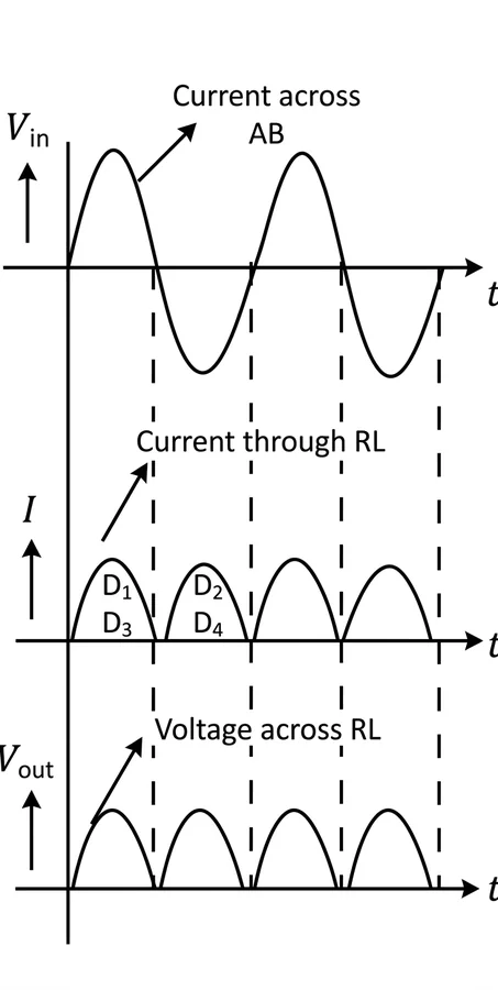
Results
The output waveform is exactly that of a full-wave rectifier, so , , ripple factor and form factor are the same as on the previous page. The only difference is that two diodes conduct in series with the load at any moment, so the resistance in the current path is :
Peak inverse voltage
PIV of a bridge rectifier. At the positive peak, D1 and D3 conduct and act almost as closed switches. Each of the non-conducting diodes D2 and D4 is then connected directly across the secondary, so it sees the peak secondary voltage in reverse: . This is half the PIV of the centre-tap circuit for the same output.
Bridge versus centre tap
Advantages of the bridge rectifier
- No centre tap is needed on the transformer.
- The whole secondary is used in both half cycles, so a much smaller transformer can be used for the same output.
- Each diode has a lower PIV rating ( instead of ), so the bridge is suitable for high-voltage applications.
- For the same secondary voltage, the output voltage is twice that of the centre-tap circuit, because the centre tap uses only half of the secondary at a time.
- Bridge rectifiers are sold as a single sealed package of four diodes, which is convenient.
Disadvantages
- Two extra diodes are needed.
- Two diodes conduct in series, so there are two diode voltage drops (about for silicon). This matters for low output voltages, and the voltage regulation is poorer.
Worked example
Example. A bridge rectifier uses diodes of forward resistance with a load of . The secondary voltage is rms. Find , and the efficiency.
Watch out. In the bridge, the diode resistance appears as (both in and in the efficiency), because two diodes conduct in series in each half cycle. In the centre-tap circuit only one diode conducts at a time, so it is .
Page 6 of 15
Comparing rectifiers, and smoothing the output
Comparison of the three rectifiers
| Half-wave | Centre-tap full-wave | Bridge | |
|---|---|---|---|
| Number of diodes | 1 | 2 | 4 |
| Diodes conducting at a time | 1 | 1 | 2 |
| (no load, ideal diode) | |||
| Maximum efficiency | 40.6 % | 81.2 % | 81.2 % |
| Ripple factor | 1.21 | 0.48 | 0.48 |
| Form factor | 1.57 | 1.11 | 1.11 |
| Peak factor | 2 | 1.414 | 1.414 |
| Ripple frequency | |||
| PIV per diode | |||
| Centre tap needed | no | yes | no |
Key idea. Full-wave rectification doubles the DC output and the efficiency and reduces the ripple factor from 1.21 to 0.48. The bridge gives the same output as the centre tap without a centre tap and with half the PIV, at the cost of two more diodes.
Advantages of full-wave over half-wave
- Efficiency is high (about 81.2 % against 40.6 %).
- Ripple factor is low (0.48 against 1.21).
- Output current is continuous but pulsating, instead of flowing only in alternate half cycles.
Disadvantages: full-wave rectifiers need two or four diodes, so the cost is comparatively high.
Why ripple matters
Even the best rectifier output (ripple factor 0.48) is far from steady DC. If such a supply powered an audio amplifier, you would hear a loud hum at . A digital circuit would reset whenever the voltage dipped. So a rectifier is almost always followed by a filter.
The capacitor filter (beyond the syllabus)
The simplest filter is a large capacitor connected directly across the load.
- As the rectified voltage rises towards its peak, the diode conducts and charges the capacitor to nearly .
- After the peak, the input falls faster than the capacitor can discharge, so the diode switches off. The capacitor now supplies the load, discharging slowly through .
- At the next pulse, the input rises above the capacitor voltage again, and the diode tops it up.
The output becomes a nearly steady DC close to , with only a small sawtooth ripple.
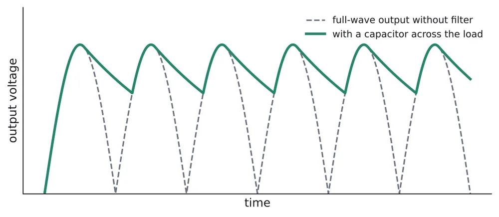
The larger and are (a long discharge time ), the smaller the ripple. For a full-wave rectifier with a capacitor filter, the ripple factor is approximately
For example, with , and , : about , compared with without the filter. (For half-wave the factor 4 becomes 2, so the ripple is twice as large.)
Watch out. The ripple factor 0.48 and the efficiency 81.2 % are for a rectifier with a resistive load and no filter. Do not write them for a filtered supply.
Page 7 of 15
Breakdown in a p-n junction
The idea
In reverse bias only a tiny reverse saturation current flows, carried by minority carriers. If the reverse voltage is increased enough, the reverse current suddenly rises steeply while the voltage hardly changes. This is breakdown, and the voltage at which it happens is the breakdown voltage. It happens in two physically different ways.
Avalanche breakdown
- It occurs in p-n junctions with lightly or moderately doped semiconductors.
- The depletion region of a lightly doped junction is wide. The breakdown voltage is relatively high (typically more than about 6 V).
- In reverse bias, the electric field accelerates the few minority carriers across the depletion region.
- As these carriers gain speed, they get enough kinetic energy, between collisions, to knock electrons out of covalent bonds. Each such collision creates a new electron-hole pair. This is called impact ionisation.
- The newly created carriers are also accelerated and in turn create more pairs, producing a chain reaction, exactly like a snow avalanche.
- This rapid multiplication of carriers causes a sudden and large increase in reverse current: avalanche breakdown.
- The large current produces heat, which can damage the diode permanently if the current is not limited by the external circuit.
- Temperature: as temperature rises, the lattice vibrates more strongly, the carriers collide more often and travel shorter distances between collisions, so they gain less energy between collisions. A higher voltage is needed to reach breakdown. So avalanche breakdown has a positive temperature coefficient.
- Use: high-voltage protection circuits (avalanche diodes).
Zener breakdown
- It occurs in p-n junctions with heavily doped semiconductors.
- The depletion region of a heavily doped junction is very thin (a few nanometres), so even a few volts of reverse bias produce an extremely strong electric field across it, of the order of .
- This field is strong enough to pull electrons directly out of their covalent bonds. In terms of bands, the valence band on the p side lines up with the empty conduction band on the n side across a very thin barrier, and electrons tunnel straight through it (quantum tunnelling, Module 2). This is also called field emission.
- The current rises sharply at a low and well-defined breakdown voltage (typically below about 6 V).
- The diode is not damaged by operating in breakdown, provided the current is kept within its power rating.
- Temperature: a higher temperature gives the valence electrons more energy, so they tunnel more easily, and the breakdown voltage falls. This is a negative temperature coefficient.
- Use: voltage regulation and reference circuits.
Comparison
| Avalanche breakdown | Zener breakdown | |
|---|---|---|
| Doping | light or moderate | heavy |
| Depletion region | wide | very thin |
| Breakdown voltage | high (above about 6 V) | low (below about 6 V) |
| Mechanism | carriers accelerated by the field knock electrons out of bonds; the new carriers do the same: a chain reaction (impact ionisation) | the very strong field pulls electrons out of bonds; they tunnel through the thin depletion region |
| Damage | can destroy the diode if the current is not controlled | the diode is not damaged in breakdown (within its power rating) |
| Effect of temperature | breakdown voltage rises (positive coefficient) | breakdown voltage falls (negative coefficient) |
| Shape of the curve | breakdown less sharp | very sharp knee |
| Use | high-voltage protection | voltage regulation and reference |
Commercial "Zener diodes" with breakdown voltages above about 6 V actually break down mainly by avalanche. Near 5 to 6 V both mechanisms act and their temperature effects nearly cancel, which is why 5.6 V reference diodes are very stable.
Note on the source. The lecture notes said that a higher temperature can lower the avalanche breakdown voltage. The usual behaviour is the opposite: stronger lattice vibrations shorten the distance carriers travel between collisions, so a higher voltage is needed, and avalanche breakdown has a positive temperature coefficient. Zener breakdown has a negative one.
Watch out. "Breakdown" does not mean the diode is broken. It is a reversible process. The diode is destroyed only if the current, and so the power , is allowed to become too large.
Page 8 of 15
The Zener diode and the voltage regulator
The Zener diode
A Zener diode is a heavily doped p-n junction diode designed to operate in the reverse breakdown region. Its breakdown voltage is set during manufacture by controlling the doping level: heavier doping gives a thinner depletion region and a lower . Zener diodes are available with from about 2 V to a few hundred volts.
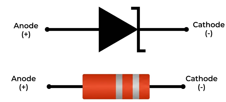
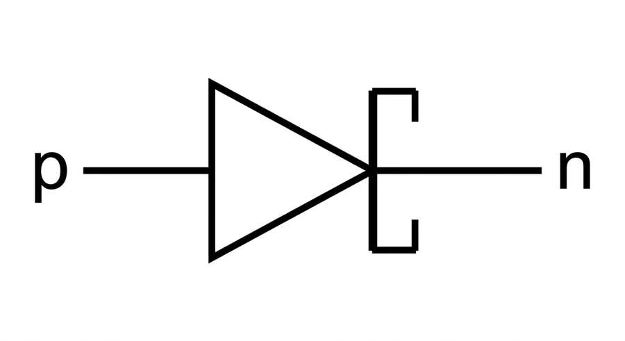
The symbol is a diode with a bent bar (like a "Z") at the cathode. On the component, the band marks the cathode.
V-I characteristic
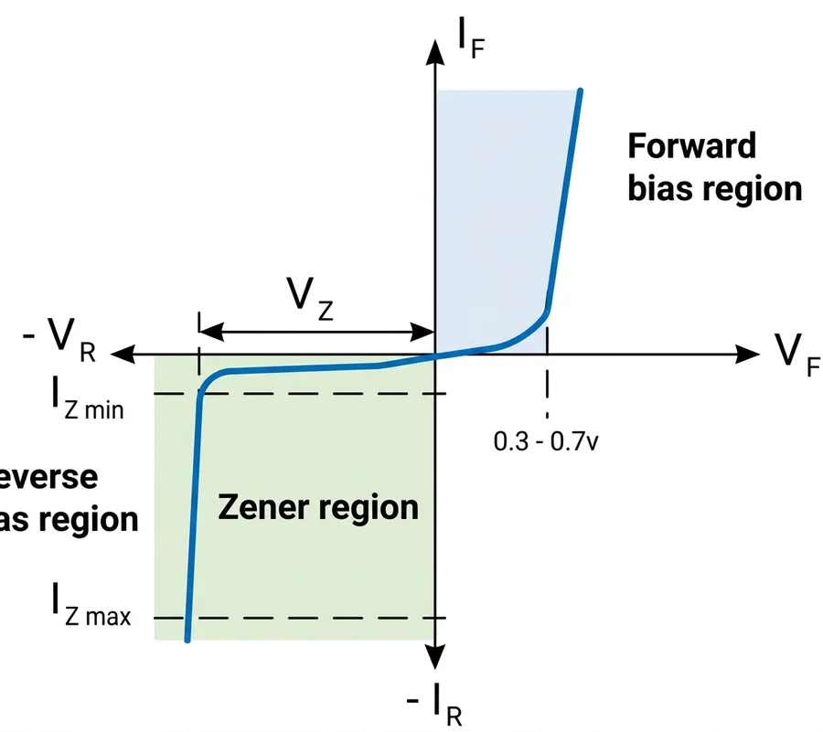
- Forward bias: the characteristic is like that of a normal p-n junction diode, conducting above about 0.3 to 0.7 V.
- Reverse bias below : only a very small reverse saturation current flows.
- At : as the reverse bias is increased to the Zener breakdown voltage, the reverse current increases sharply, while the voltage across the diode stays almost constant at . The curve is nearly vertical.
- (knee current): the smallest current at which the diode is properly in breakdown. Below it the voltage is no longer held at .
- : the maximum reverse current the diode can carry without exceeding the power dissipation rating given by the manufacturer: .
Key idea. Between and the Zener voltage stays almost constant whatever the current. A device that holds its voltage while the current changes is exactly what a voltage regulator needs.
Zener diode as a voltage regulator
A regulated power supply keeps its output voltage constant, irrespective of changes in the input supply voltage or in the load resistance.
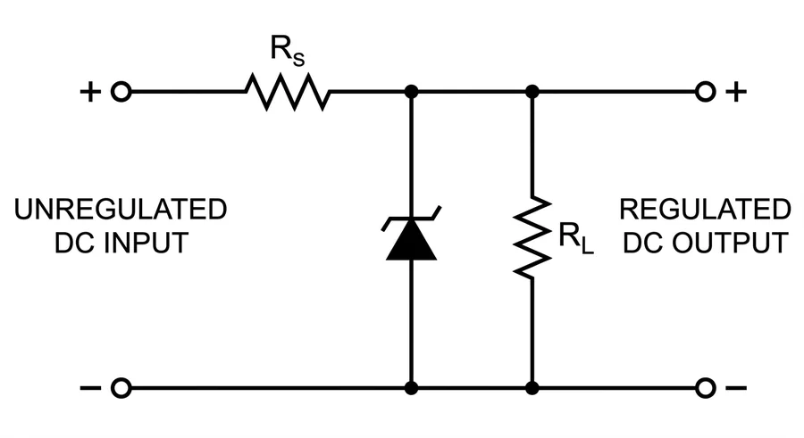
Circuit. The unregulated DC input is applied through a series resistor . The Zener diode is connected in reverse bias, in parallel with the load , so the load voltage is the Zener voltage.
Currents. The current through divides between the Zener and the load:
How it regulates.
- If the input voltage rises: increases. The load voltage cannot rise, because the Zener holds it at . The extra current goes through the Zener and the extra voltage is dropped across . If the input falls, the Zener current falls instead.
- If the load draws more current ( falls): stays the same (since and have not changed), so the Zener current falls by the same amount and the load voltage does not change.
In both cases the output stays at , as long as the Zener current stays between and .
Role of . It limits the current, so that the Zener current never goes above , and it drops the difference between and . Without it, the Zener would be connected straight across the supply and would burn out.
Worked examples
Example 1. A Zener regulator has , , and . Find the currents and the power dissipated in the Zener. What happens if rises to ?
At : , is still , so . The extra flows through the Zener and the output stays at .
Example 2 (design). Design a regulator to give from an input that varies between and , for a load current between and . The Zener has and needs .
must be small enough that in the worst case (lowest input, largest load) the Zener still gets :
must be large enough that in the other worst case (highest input, no load) the Zener current stays below :
Choose a standard value between them, . Check: at with no load, and . At with load, .
Watch out. The Zener diode is connected in reverse bias in the regulator, with its cathode to the positive side. In forward bias it would just be an ordinary diode with a 0.7 V drop. Also, the load is in parallel with the Zener, not in series.
Page 9 of 15
The tunnel diode
The idea
The tunnel diode (also called the Esaki diode, after Leo Esaki, who invented it in 1957 and later shared the Nobel Prize) is a p-n junction diode with very heavy doping on both sides, about a thousand times heavier than an ordinary diode.
The heavy doping has two consequences:
- The depletion region is extremely narrow, about or less.
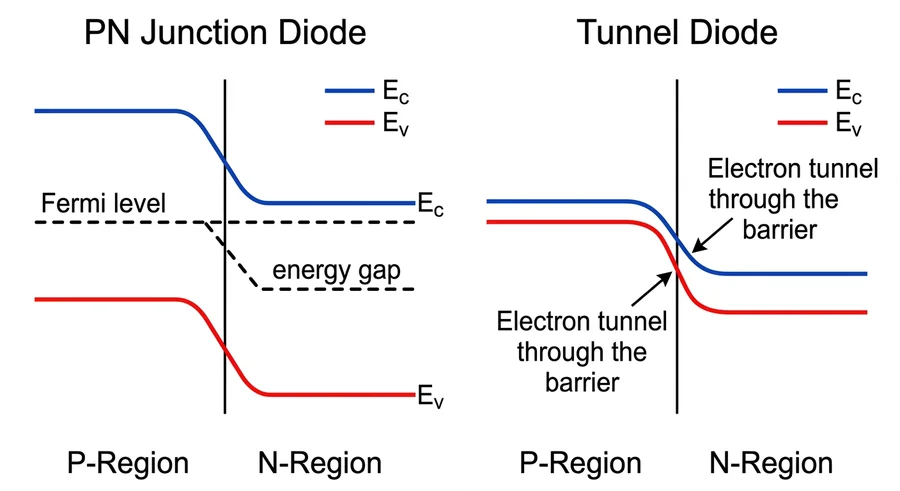
- The material is degenerate: the Fermi level lies inside the conduction band on the n side and inside the valence band on the p side.
Electrons can then cross the junction by quantum mechanical tunnelling (Module 2) straight through the thin barrier, instead of climbing over it. Tunnelling happens only from a filled state on one side into an empty state at the same energy on the other side.
Working, point by point on the V-I curve
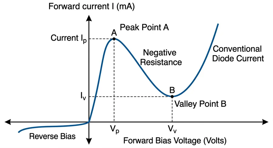
1. Zero bias. The Fermi levels on the two sides are aligned. Filled states in the n-side conduction band face filled states in the p-side valence band. Tunnelling occurs equally in both directions, so the net current is zero.
2. Small forward bias. The n side is raised relative to the p side. Filled states in the n-side conduction band now face empty states (holes) in the p-side valence band at the same energy. Electrons tunnel from n to p and the current rises rapidly with voltage, much faster than in an ordinary diode.
3. Peak point A (, ). The overlap between filled conduction-band states on the n side and empty valence-band states on the p side is largest. The tunnelling current is maximum: the peak current at the peak voltage (typically about to ).
4. Negative resistance region (A to B). As the forward bias increases further, the bands are pushed out of alignment. Fewer filled states on the n side face empty states on the p side, so tunnelling decreases and the current falls while the voltage rises. The slope is negative: this is the negative resistance region.
5. Valley point B (, ). The bottom of the n-side conduction band has risen above the top of the p-side valence band. There are no empty states opposite the filled ones, so tunnelling stops. The current is at its minimum, the valley current , at the valley voltage (typically a few tenths of a volt).
6. Beyond the valley. The forward bias is now large enough for carriers to cross the reduced barrier by the ordinary diffusion mechanism. Normal diode conduction takes over and the current rises again exponentially.
7. Reverse bias. Filled states in the p-side valence band face empty states in the n-side conduction band, so electrons tunnel from p to n. The reverse current rises rapidly even for a tiny reverse voltage. A tunnel diode conducts well in reverse and is not used as a rectifier.
Key idea. The negative resistance region is what makes the tunnel diode useful. A device whose current falls as the voltage rises can supply AC power to a resonant circuit (taking it from the DC bias), so it can sustain oscillations and amplify.
Example. A tunnel diode has at and at . Estimate its average negative resistance.
Advantages and applications
Advantages: very fast (tunnelling is almost instantaneous, so it works at very high frequencies), low noise, low power consumption, simple and cheap, and relatively insensitive to temperature and radiation.
Applications
- High-frequency oscillators (in the GHz range), using the negative resistance.
- Microwave amplifiers.
- High-speed switching circuits.
- Radar and communication systems.
- Logic memory (storage) devices, using its two stable states.
Watch out. "Negative resistance" means the current falls as the voltage rises between the peak and valley points. It does not mean the diode produces energy. The power comes from the DC bias supply.
Page 10 of 15
The light-emitting diode (LED)
The idea
A light-emitting diode (LED) is a semiconductor p-n junction diode that gives out light when it is forward biased. It converts electrical energy directly into light, a process called electroluminescence.
Working
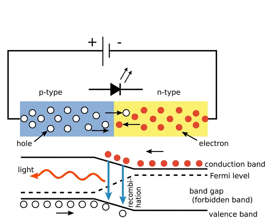
- Under forward bias the barrier is lowered. Free electrons cross from the n region into the p region, and holes cross in the opposite direction.
- Near the junction, these minority carriers recombine with the majority carriers: electrons fall into holes.
- Free electrons are in the conduction band, and holes are in the valence band, which is lower in energy. So each recombination releases energy, roughly equal to the band gap .
- This energy is released either as heat (lattice vibrations) or as light (a photon of energy ).
- If the semiconductor is translucent, the light comes out and the junction becomes a light source.
Direct and indirect band gaps
Why do some diodes give light while silicon diodes only get warm?
- In a direct band gap material (GaAs, GaAsP, GaP with nitrogen, GaN, InGaN), the lowest point of the conduction band and the highest point of the valence band occur at the same electron momentum. An electron can drop straight down into a hole and emit a photon, which carries away the energy. This is radiative recombination, and it is fast and likely.
- In an indirect band gap material (silicon and germanium), they occur at different momenta. A photon carries almost no momentum, so the electron cannot drop by emitting a photon alone. A lattice vibration (phonon) must also take part. This is much less likely, so recombination usually happens without light, and the energy is released as heat.
That is why LEDs and laser diodes are made from compound semiconductors, not from silicon.
Colour and band gap
The photon energy is about , so the wavelength emitted is
With this becomes the handy formula
A larger band gap gives a shorter wavelength (towards blue); a smaller gap gives a longer wavelength (towards red and infrared). Different colours are obtained by choosing the material, and by adjusting the composition of alloys such as GaAsP.
| Material | Approximate | Approximate | Light |
|---|---|---|---|
| GaAs | 1.43 eV | 870 nm | infrared (remote controls) |
| GaAsP | about 1.9 eV | about 650 nm | red |
| AlGaInP | about 2.1 eV | about 590 nm | yellow and amber |
| GaP | 2.26 eV | about 550 nm | green |
| InGaN | about 2.75 eV | about 450 nm | blue |
| GaN | 3.4 eV | about 365 nm | ultraviolet |
White LEDs use a blue InGaN chip coated with a phosphor that changes part of the blue light to yellow. Blue plus yellow looks white.
Advantages and applications
Advantages: low operating voltage (about 1.5 to 3.5 V) and current; long life (tens of thousands of hours); high efficiency compared with filament lamps; very fast switching (nanoseconds); small, strong and available in many colours.
Disadvantages: output falls with rising temperature; needs a current-limiting resistor; can be damaged by reverse voltage or excess current.
Applications: indicator lamps and seven-segment displays; general lighting and torches; remote controls (infrared LEDs); optical fibre communication over short distances; traffic signals and vehicle lights; backlights for LCD screens; optocouplers.
Worked examples
Example 1. Find the photon energy of red light of wavelength .
Example 2. A red LED needs at . Find the series resistor to run it from a supply.
Watch out. In , must be in electron volts and the answer comes in micrometres. For example, gives .
Page 11 of 15
Photodetectors: p-n and PIN photodiodes
The idea
Photodetectors are devices that change incident light power into an electrical signal (current). They are the receivers in optical fibre links, the sensors in cameras and light meters, and the "eyes" of automatic doors and smoke detectors.
What a good photodetector needs
- Wide bandwidth: it should detect light over a wide range of frequencies (wavelengths).
- Low response time: it should respond quickly to changes in the light.
- Sharp response: to handle high bit rates in communication.
- Long operating life.
- Low cost.
- Small size.
- High degree of temperature tolerance.
- High sensitivity: a large output for a small light input.
The p-n junction photodiode
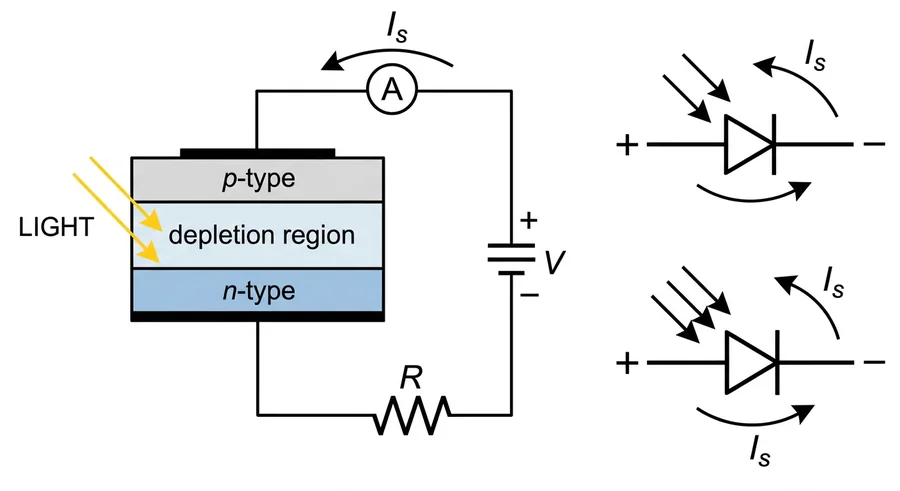
Structure. A photodiode is essentially a p-n junction diode, built so that light can reach the junction (through a window or a lens) and operated in reverse bias.
Without light. During fabrication a depletion layer forms at the junction, made of immobile negative acceptor ions on the p side and positive donor ions on the n side. The field of these ions stops the majority carriers but accelerates minority carriers across the junction. A reverse bias widens the depletion region. The motion of the thermally generated minority carriers gives a small reverse leakage current even in complete darkness. This is the dark current.
With light.
- Light falls on the diode and photons are absorbed, mainly in the depletion region but also in the neutral regions.
- A photon of energy lifts an electron from the valence band to the conduction band, leaving a hole. These electron-hole pairs are called photocarriers.
- A pair created in the depletion region is separated at once by the field there: the electron drifts to the n side and the hole to the p side.
- This movement produces a current in the external circuit in excess of the dark current, called the photocurrent.
- Pairs created in the neutral regions diffuse slowly. Many recombine before reaching the depletion region and give nothing.
Cut-off wavelength. Only photons with can create pairs, so there is a longest wavelength the diode can detect:
For silicon (), . For germanium (), it is about .
V-I characteristic
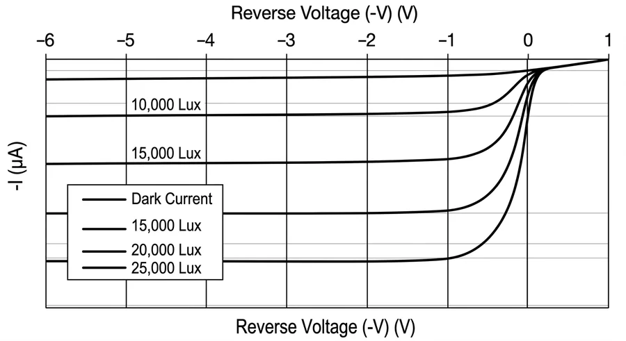
- The photocurrent always flows in the reverse direction, from n to p.
- With no light only the small dark current flows.
- If the illumination is increased, the reverse current increases in proportion to the light intensity.
- Once the reverse bias is more than a fraction of a volt, the current hardly depends on the voltage. Each curve is almost flat.
Because the photocurrent is proportional to the incident light intensity, the reverse-biased diode can be used as a photodetector.
Drawbacks of the p-n photodiode
- The depletion region is only a small part of the volume of the diode. Only photons absorbed there produce current. Photons absorbed in the bulk of the diode are mostly wasted.
- The depletion region can be widened by increasing the reverse bias, but only up to a limit set by breakdown.
- Electron-hole pairs generated in the bulk recombine before they can contribute to the current, and the slow diffusion of those that survive makes the response slow.
The PIN photodiode
Structure. A p-i-n diode has a wide layer of intrinsic (pure or very lightly doped) semiconductor between the p and n regions. The intrinsic layer has very few free carriers, so under a modest reverse bias the depletion region spreads through the whole intrinsic layer. So the region that collects light is much wider.
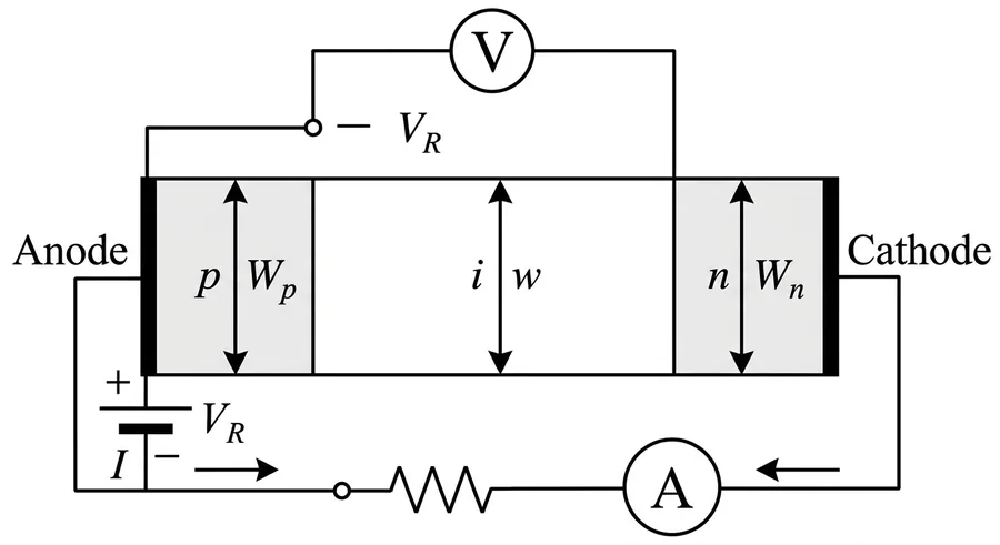
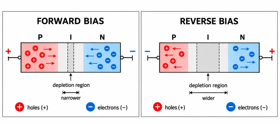
Working. A photon with energy at least that reaches the wide depletion region lifts an electron from the valence band to the conduction band, creating a free electron-hole pair. The high electric field across the intrinsic layer separates the carriers quickly and they drift to the contacts, producing a current in the external circuit. Because the intrinsic layer is wide, most photons are absorbed there and a much larger photocurrent is produced. So a PIN photodiode is more sensitive than a p-n photodiode.
Advantages of the PIN photodiode
- The depletion region is wide and extends through the whole intrinsic region, so the reverse bias need not be increased to widen it.
- The reverse bias required is small, of the order of .
- As the depletion region is wide, most incident photons are absorbed in it, so the efficiency is high.
- The dark current is small.
- Carriers are collected by fast drift instead of slow diffusion, so the response is fast.
p-n versus PIN photodiode
| p-n photodiode | PIN photodiode | |
|---|---|---|
| Structure | p and n regions only | wide intrinsic layer between p and n |
| Depletion region | narrow | wide: fills the intrinsic layer |
| Photons collected | only those absorbed in the narrow depletion region | most incident photons |
| Sensitivity and efficiency | lower | higher |
| Response speed | slower (much diffusion) | faster (mostly drift) |
| Reverse bias needed to widen depletion region | large | small (about 5 V) |
| Dark current | larger | smaller |
Two measures of performance (beyond the syllabus)
The responsivity (amperes of photocurrent per watt of light) and the quantum efficiency (electrons collected per incident photon) are related by .
Example. A photodiode gives for of light at . Then and : 73 % of the photons produce an electron.
Watch out. Photodiodes are operated in reverse bias, and the photocurrent is a reverse current. Solar cells (next page) are not biased at all: they produce their own voltage.
Page 12 of 15
Solar cells
The idea
A solar cell (photovoltaic cell) is a semiconductor p-n junction device that converts the energy of light, usually sunlight, directly into electrical energy. Unlike a photodiode it needs no external bias: it generates its own voltage, which depends on the intensity of the incident light. Materials used include silicon (by far the most common), selenium, GaAs, InAs and CdS.
Construction
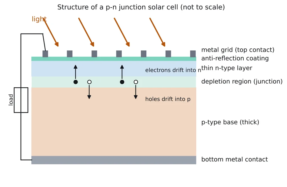
- A p-type silicon chip forms the thick base.
- A thin n-type layer is grown or diffused on top, so that light can reach the junction just below the surface.
- The top surface has an anti-reflection coating (so that less light is reflected away) and a fine metal grid contact (a grid instead of a full sheet, so that light gets through).
- The bottom surface has a full metal contact.
- A load is connected between the top and bottom contacts.
Working, step by step
- Absorption. Photons with energy greater than are absorbed in the n and p regions and near the junction, creating electron-hole pairs.
- Diffusion to the junction. Pairs created within about one diffusion length of the junction reach the depletion region before recombining.
- Separation. The built-in electric field of the immobile ions in the depletion region separates each pair: electrons are pushed into the n region and holes into the p region. (Minority electrons in the p region are drawn into the n region, and minority holes in the n region into the p region.)
- Photo-emf. Electrons collect on the n side and holes on the p side, so the n side becomes negative and the p side positive. This produces a potential difference across the cell, the photo-voltage or photo-emf.
- Current. If a load is connected, the collected charges flow round the external circuit and deliver power. The power depends on the material, the light intensity and the load resistance.
I-V characteristic
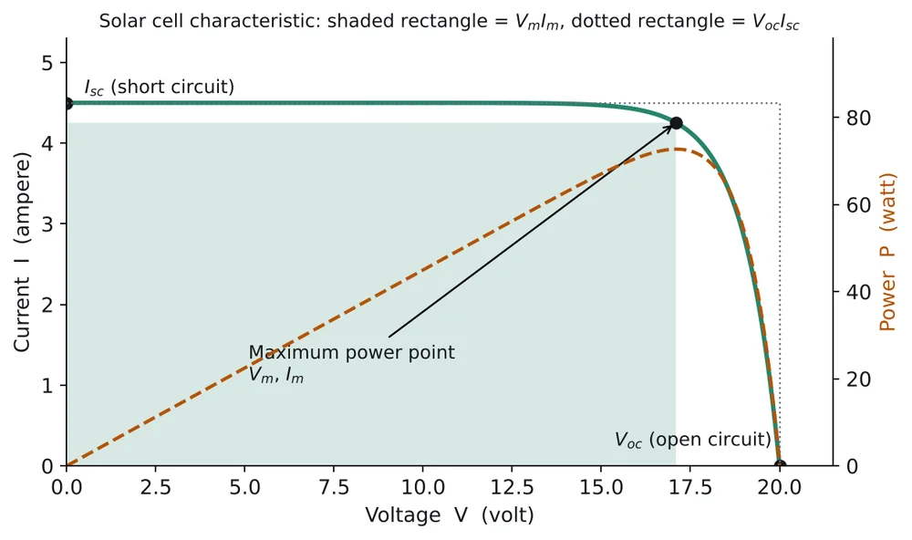
- Short-circuit current : the current when the terminals are shorted (voltage zero). It is proportional to the light intensity.
- Open-circuit voltage : the voltage across the illuminated cell when no current is drawn (open circuit). For a silicon cell it is about to , and it increases only slowly (logarithmically) with intensity.
- Between them, the current stays nearly constant at about until the voltage comes close to , and then drops steeply.
- The power delivered is . At both ends of the curve, open circuit and short circuit, the power is zero. In between it rises to a maximum at the maximum power point, with voltage and current , at the "knee" of the curve. The load should be chosen so that the cell works at this point.
Efficiency
Conversion efficiency. The ratio of the maximum electrical output power to the light power falling on the cell:
Commercial silicon cells reach about 15 to 22 %. The losses come from photons with too little energy to create a pair, the excess energy of energetic photons lost as heat, reflection, recombination and resistance.
Fill factor
The fill factor tells what fraction the maximum power is of the product of open-circuit voltage and short-circuit current. On the graph, it is how much of the dotted rectangle () is filled by the shaded maximum-power rectangle (). A squarer I-V curve gives a higher fill factor. Its value is usually between 0.65 and 0.8. The higher the fill factor, the greater the output power for the same and .
Example. A silicon cell of area in sunlight of has , , and its maximum power point at , . Find the fill factor and the efficiency.
Stringing cells into modules, panels and arrays
One silicon cell gives only about and a few amperes, so cells are connected together:
- Connecting cells in series adds their voltages (the current is the same through all).
- Connecting cells (or strings) in parallel adds their currents (the voltage is the same).
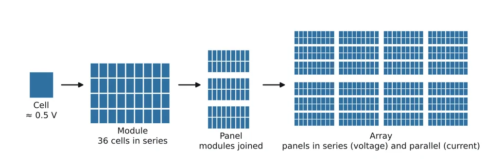
| Level | What it is |
|---|---|
| Cell | a single p-n junction, about |
| Module | cells connected in series and sealed in one frame; a typical module has 36 cells in series, giving about at the maximum power point (enough to charge a 12 V battery) |
| Panel | several modules mounted and wired together as one unit |
| Array | many panels connected in series (for a higher voltage) and in parallel (for a higher current) to give the power required |
Example. Each cell of a module has and . (a) Find the output of a module of 36 cells in series. (b) How many such modules are needed for a , array, and how are they connected?
(a) Series cells add voltage: at , so the module gives .
(b) For , put modules in series in each string; one string gives . For we need strings in parallel: 40 modules in all, giving at .
In practice, a shaded cell in a series string limits the current of the whole string, so modules include bypass diodes that let the current go round shaded cells.
Advantages, disadvantages and applications
| Advantages | Disadvantages |
|---|---|
| does not use any fuel, so not dangerous | very delicate and brittle; can break into pieces |
| can be used for years with almost no maintenance cost | slow response compared with photodiodes, so not used as photodetectors |
| produces no atmospheric or noise pollution | needs a large area for useful power |
| must be cleaned from time to time for maximum output | |
| output only while the light falls; storage is needed at night |
Applications
- Power for satellites and rockets.
- Telecommunications in remote and inaccessible areas.
- Defence equipment, remote instrumentation and remote radars.
- Rural electrification, water pumping, solar fencing, health care and ocean navigation aids.
- Pocket calculators, watches, street lights and traffic signals.
Photodiode versus solar cell
| Parameter | Photodiode | Solar cell |
|---|---|---|
| Junction area | smaller | larger, as solar radiation must fall on a large area to give useful power |
| Biasing | a reverse bias voltage is applied externally | no voltage is applied: it generates its own |
| Size | small | large |
| Load capacity | smaller | greater |
| Application | used as a light sensor, to detect the presence of light | used as a transducer, to convert light energy into electrical energy |
Watch out. Efficiency compares output power with the light power falling on the cell (intensity × area), not with . The fill factor is the ratio with . Also remember to change the area to square metres when the intensity is in .
Page 13 of 15
The semiconductor laser
What a laser needs
LASER stands for Light Amplification by Stimulated Emission of Radiation. Light can interact with matter in three ways:
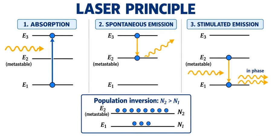
- Absorption. An atom (or electron) in a lower level absorbs a photon and jumps to a higher level.
- Spontaneous emission. An excited electron falls back on its own, at a random moment, emitting a photon in a random direction and with random phase. Light from lamps and LEDs is of this kind: incoherent.
- Stimulated emission. A photon of the right energy passing an excited electron triggers it to fall, emitting a second photon identical to the first: same frequency, same phase, same direction and polarisation. One photon becomes two, two become four. The light is amplified and coherent.
Normally there are more electrons in the lower level than in the upper one, so absorption is more than stimulated emission. A laser needs three things:
| Requirement | Meaning | How a diode laser achieves it |
|---|---|---|
| Population inversion | more electrons in the upper level than in the lower (), so stimulated emission wins | heavy doping and a large forward current |
| Pumping | a source of energy that keeps the inversion going | the forward current itself: direct injection of carriers from a DC supply |
| Optical feedback (resonator) | mirrors that send the light back and forth through the active region, building up stimulated emission | the polished end faces of the crystal |
The diode laser
A semiconductor diode laser is a specially made p-n junction diode that emits coherent light when forward biased. The first semiconductor laser was made in 1962 by R. N. Hall and his co-workers.
Silicon and germanium, used for ordinary diodes, are indirect band gap materials and produce only heat when electrons and holes recombine. A laser needs light, so it is made from a direct band gap material such as GaAs.
- A homojunction laser uses the same semiconductor on both sides of the junction, for example a GaAs laser. We study this one.
- A heterojunction laser uses different semiconductors on the two sides, for example GaAs on one side and GaAlAs on the other. The different materials confine the carriers and the light to a thin active layer, which lowers the threshold current enormously. Nearly all practical diode lasers today are heterojunction lasers.
Construction (GaAs homojunction laser)
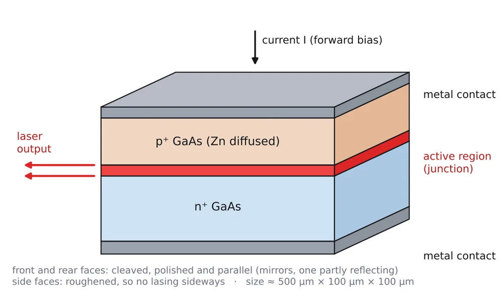
- A heavily doped n-type GaAs crystal, on top of which a heavily doped p region is formed by diffusing zinc atoms into it. The junction between them is the active region.
- The diode is tiny: typically .
- The top and bottom faces are metallised, with metal contacts to pass current through the junction.
- The front and rear end faces are cleaved and polished parallel to each other and perpendicular to the plane of the junction, one fully reflecting and the other partially reflecting. Together they form the optical resonator (a Fabry-Perot cavity). Even an uncoated GaAs face reflects about 32 % of the light, because GaAs has a high refractive index (about 3.6).
- The two remaining side faces are roughened, so that light is not reflected back along those directions and lasing cannot occur sideways.
- The whole structure is packed in a small case, usually with a heat sink.
Working
- Heavy doping. Because of the heavy doping, the n region has a very large number of electrons in its conduction band and the p region has a very large number of holes in its valence band.
- Pumping by forward bias. When the junction is forward biased, electrons from the n side and holes from the p side are injected into the narrow junction region in very high concentration. This is the pumping. It is done directly by the DC voltage source, by direct transfer of electrical energy.
- Population inversion. The junction region now has a large population of electrons in the conduction band and, at the same place, a large population of holes, which are empty states, in the valence band. Since a hole is the absence of an electron, there are more electrons in the high-energy conduction band than in the corresponding states of the low-energy valence band. This is population inversion. The narrow region where this happens is the inversion region or active region.
- Spontaneous emission. Chance recombination of electrons and holes produces spontaneous photons with energy , travelling in all directions. Below threshold, the diode simply behaves as an LED.
- Threshold and stimulated emission. When the diode current reaches a threshold value, the gain from stimulated emission becomes more than the losses. Spontaneous photons travelling in the plane of the junction stimulate conduction electrons to fall into the holes of the valence band, each emitting a photon identical to the stimulating one.
- Amplification in the resonator. These photons are reflected back and forth between the polished end faces, passing through the active region again and again and stimulating more emission each time. Photons travelling in other directions leave the active region and are lost.
- Output. A strong, coherent, monochromatic beam comes out through the partially reflecting face. For GaAs, (near infrared).
Above threshold the light output rises steeply and linearly with current.
Salient features
- High efficiency: a large fraction of the electrical input becomes light.
- Simple, compact and small in size.
- Low input power and low operating voltage.
- Output power can be controlled simply by controlling the junction current, so the light can be modulated at very high speed (useful for communication).
- Can work as a continuous-wave laser (heterojunction devices do so at room temperature).
Compared with gas and solid-state lasers, the beam is more divergent and the spectrum is somewhat wider.
Applications
- Optical fibre communication (the main light source).
- CD, DVD and Blu-ray players and recorders.
- Laser printers and barcode scanners.
- Laser pointers and range finders.
- Medical instruments and laser surgery.
- Pumping other lasers.
Example. A diode laser emits at . How many photons does it emit per second?
LED versus laser diode
| LED | Laser diode | |
|---|---|---|
| Emission | spontaneous | stimulated (above threshold) |
| Light | incoherent | coherent |
| Spectrum | broad (tens of nm) | very narrow |
| Beam | spreads widely | narrow, directional |
| Population inversion | not needed | essential |
| Optical resonator | none | polished end faces |
| Threshold current | none: light at any forward current | light output rises sharply above threshold |
| Uses | displays, lighting, short-distance links | long-distance fibre links, optical discs, printers |
Watch out. An LED and a laser diode both emit light from recombination at a forward-biased junction. The difference is that the laser has population inversion, an optical resonator and works above a threshold current, so its light is stimulated and coherent. The light of an LED is spontaneous and incoherent.
Page 14 of 15
Numerical problems
These are the problems from the lecture notes, worked in full and checked again.
Problem 1. A half-wave rectifier is used to supply DC to a resistive load of . The diode has a forward resistance of . Find the peak AC input voltage required.
Given , , . Since with and :
Problem 2. A half-wave rectifier is connected to a step-down transformer whose output is (rms), . The load resistance is and the diode resistance is . Find (1) the average load current, (2) the rms load current, (3) the DC output voltage.
Problem 3. In a full-wave single-phase (centre-tap) rectifier, the internal resistance of each diode is , the transformer secondary voltage from the centre tap to each anode is rms, and the load resistance is . Find the mean load current, the rms load current and the DC output power.
- Mean load current:
- RMS load current:
- DC output voltage:
- DC output power:
Note on the source. The lecture notes gave , but is . They also did not calculate the DC output power, which the question asks for.
Problem 4. A half-wave rectifier has volts, and . Find (1) the average load current, (2) the DC output voltage, (3) the PIV.
Problem 5. The forward resistance of each diode in a centre-tap full-wave rectifier is . The transformer secondary voltage from the centre tap to each end is rms and the load resistance is . Find (1) the average load current, (2) the rms load current, (3) the efficiency.
Check with the formula: .
Problem 6. A light-emitting diode emits light of wavelength when forward biased. What is the band gap of the material of the diode?
(violet light, from a wide band gap material such as InGaN).
Watch out. Always change rms to peak first (), and include the diode resistance in ( for a bridge). Using the rms voltage directly is the most common mistake in these problems.
Page 15 of 15
Practice questions and formula sheet
Practice questions
- A full-wave rectifier gives . What is , and what is ?
- Find the wavelength emitted by a GaAs LED with . In which part of the spectrum is it?
- A solar cell of area receives light of intensity . At its maximum power point and . Also and . Find the efficiency and the fill factor.
- Find the ripple factor of a half-wave rectifier from its form factor.
- A Zener regulator has , , . Find the Zener current with no load, and the power it dissipates.
- What is the longest wavelength a silicon photodiode () can detect?
Answers
- , and .
- : infrared.
- Input power . Output , so . .
- Form factor , so .
- With no load, all of goes through the Zener: , .
- .
Short questions to revise
- Explain the working of a half-wave rectifier and derive its efficiency and ripple factor.
- Draw the centre-tap full-wave rectifier and explain its working with waveforms. Why is its PIV ?
- Explain the working of a bridge rectifier. Compare it with the centre-tap rectifier.
- Define ripple factor, form factor and rectifier efficiency.
- Distinguish between avalanche and Zener breakdown.
- Draw the V-I characteristic of a Zener diode and explain how it regulates voltage.
- Explain the V-I characteristic of a tunnel diode using band diagrams. What is negative resistance?
- Why do silicon diodes not emit light, while GaAs diodes do?
- Compare p-n and PIN photodiodes.
- Explain the working of a solar cell. Define fill factor and efficiency, and explain how cells are connected to form a panel.
- Describe the construction and working of a semiconductor laser. How does it differ from an LED?
Formula sheet
Rectifiers
| Half-wave | Full-wave (centre tap) | Bridge | |
|---|---|---|---|
| Efficiency | |||
| Ripple factor | 1.21 | 0.48 | 0.48 |
| Form factor | 1.57 | 1.11 | 1.11 |
| PIV |
| Efficiency | |
| Ripple factor | |
| DC output voltage | |
| Peak from rms | |
| Capacitor filter (full-wave) |
Zener regulator
| Series current | |
| Load and Zener currents | , |
| Maximum Zener current | |
| Limits on |
Photonic devices
| LED wavelength | |
| Photodiode cut-off | |
| Solar cell efficiency | |
| Fill factor | |
| Cells in series / parallel | voltages add / currents add |
| Photons per second |