
Nanomaterials: scale, classification and size effects
Nanomaterials
Nanomaterials are materials with at least one external dimension or internal structural feature in the nanometric range, conventionally defined as approximately to , where . While some structures such as monolayer graphene have a thickness below (), they are still studied as nano-objects because their thickness is at the atomic limit. Nanomaterials can occur naturally (volcanic ash, forest fire soot), form as incidental combustion by-products (diesel exhaust, welding fumes), or be engineered for specific electronic, optical, or catalytic functions.
Nanoscience
Nanoscience investigates the fundamental physical, chemical, and biological phenomena of matter at the atomic and molecular scale.
Nanochemistry
Nanochemistry focuses on synthesizing, functionalizing, and controlling chemical reactions of nanoscale building blocks with molecular precision.
Nanotechnology
Nanotechnology applies these scientific and chemical principles across engineering, physics, and materials science to fabricate functional devices.
Classification by dimensionality
In nanomaterial classification, dimensionality (, , , ) counts the number of unconfined (extended) spatial axes that lie outside the nanometric range (), rather than the number of nanoscale axes.
| Class | Confined axes () | Unconfined axes () | Typical morphology and examples |
|---|---|---|---|
| 0D | 3 | 0 | All three dimensions are confined at the nanoscale: spherical nanoparticles, semiconductor quantum dots, nanoclusters, and fullerenes (). |
| 1D | 2 | 1 | Elongated along one axis with nanoscale cross-sections: nanorods, nanowires, nanofibres, and carbon nanotubes (CNTs). |
| 2D | 1 | 2 | Extended sheets or films with nanoscale (or sub-nanometre) thickness: graphene, nanofilms, nanocoatings, and layered nanoplates. |
| 3D | 0 (external) | 3 | Bulk-scale external dimensions composed of nanoscale internal building blocks, grains, pores, or interfaces: nanocrystalline polycrystals, nanoparticle dispersions, and bundled nanowire arrays. |
Watch out. Do not assume any macroscopic solid with all three external dimensions above is a nanomaterial. Ordinary bulk materials (such as coarse-grained graphite) are not nanomaterials unless they possess a nanostructured internal architecture, such as nanometre-scale crystal grains, pores, or bundled nano-building blocks.
Classification by material composition
Grouping nanomaterials by chemical composition is a material-type classification rather than a commercial grading, and several categories overlap in practice (for example, a polymer nanocomposite contains both polymer and inorganic phases).
| Material category | Core composition and structural features | Representative examples |
|---|---|---|
| Carbon-based | Predominantly or bonded carbon nanostructures. | Fullerenes, carbon nanotubes (CNTs), graphene, carbon quantum dots. |
| Inorganic: metals, oxides and semiconductors | Metallic nanoparticles, metal-oxide nanopowders, or compound semiconductor nanocrystals. | , , and nanoparticles; oxides such as , , , , ; quantum dots such as and . |
| Dendrimers (branched nanopolymers) | Radially branched, tree-like macromolecular architectures containing internal cavities and numerous functionalizable chain ends for targeted drug delivery. | Poly(amidoamine) (PAMAM) dendrimers. |
| Biological nanomaterials | Nanostructures derived from or assembled using biomolecules for bionanotechnology and targeted delivery. | DNA nanostructures/nanowires, nanostructured peptides. |
| Nanocomposites | Multiphase materials combining nanoscale fillers (, , or ) within a bulk metal, ceramic, or polymer matrix to enhance mechanical, thermal, or barrier properties. | Polyethylene–nano- composites, polymer–nanoclay systems. |
Watch out. Not all nanopolymers are dendrimers—dendrimers are a specific hyperbranched class with tree-like symmetry, whereas polymeric nanoparticles can also be formed from linear chains. Furthermore, "biological" origin does not automatically guarantee biocompatibility or non-toxicity; every nanomaterial requires specific toxicological assessment.
Size effects: governing mechanisms
Entering the range does not automatically improve every property, nor does a single universal percentage of surface atoms apply to all materials at a given diameter (surface atom fraction depends on crystal lattice parameters and particle shape). However, two fundamental physical mechanisms govern why nanomaterials differ from bulk solids:
- Surface-area-to-volume ratio (): For a sphere of diameter , surface area is and volume is . For a cube of side length , and . Their surface-to-volume ratios are:
where and are characteristic lengths ( or ). Because scales inversely with size (), subdividing a fixed total mass of material into smaller, non-agglomerated particles of identical geometry and density increases the total exposed surface area proportionally to . A much higher fraction of atoms sits at under-coordinated surface sites, which can change reactivity, catalytic activity, adsorption and melting behaviour. The result depends on material chemistry, surface state and environment.
- Electronic and optical confinement: When particle dimensions approach the de Broglie wavelength of charge carriers or the exciton Bohr radius, quantum confinement restricts electron motion. This occurs most prominently in semiconductor quantum dots (such as ), where shrinking the crystal discretizes energy levels and widens the band gap, shifting optical absorption and fluorescence toward shorter (bluer) wavelengths. By contrast, in metallic nanoparticles (such as and ), optical changes across the range are typically dominated by localized surface plasmon resonance (LSPR)—the collective oscillation of conduction electrons driven by light—rather than semiconductor-type band-gap opening, unless metallic clusters shrink to sub- molecular scales.
Example 1: Illustrative calculation of surface scaling on subdividing spheres
Problem: Consider an idealized, non-agglomerated sample of spherical nanoparticles of uniform density. If a single spherical particle of diameter is subdivided into smaller spherical particles of diameter while conserving total material volume, determine: (a) how the surface-to-volume ratio changes, (b) how the surface area of a single particle changes, (c) how many particles are formed, and (d) how the total surface area of the fixed volume changes.
Solution:
- Assumptions: All particles are perfect rigid spheres of constant density with no clustering or pore overlap.
- (a) Surface-to-volume ratio (): Using :
The surface-to-volume ratio increases by a factor of .
- (b) Surface area of one particle: Since , reducing diameter by reduces the area of an individual sphere by a factor of (), rather than increasing it.
- (c) Number of particles () at constant total volume: Since :
- (d) Total surface area () at constant volume:
Subdividing the same volume of material from to spheres increases the total exposed surface area -fold.
Self-check questions
- Question: A carbon nanotube has a diameter of and a length of . How is it classified by dimensionality, and why? Answer: It is a nanomaterial because two of its dimensions (the cross-sectional axes, ) are confined within the nanometric range, leaving exactly one unconfined dimension () extended outside the nanoscale.
- Question: Why does a nanocrystal emit a different colour of light than a nanocrystal of the exact same chemical formula? Answer: Due to quantum confinement, restricting excitons within the smaller semiconductor crystal widens the electronic band gap compared to the crystal, causing it to emit higher-energy (shorter-wavelength) photons upon electron–hole recombination.
Module study map
- Nanomaterials: scale, classification and size effects
- Nanoparticle synthesis: reduction, hydrolysis and sol–gel
- Graphene: structure, preparation, properties and uses
- Fullerenes and the structure of C₆₀
- Carbon nanotubes: structure, chirality and applications
- Carbon quantum dots and applications of nanomaterials
- Polymer fundamentals and flame retardancy
- Conducting polymers: conjugation, doping and composites
- Polyaniline and polypyrrole: preparation, states and uses
- OLEDs: layers, charge injection and light emission
- Dye-sensitized solar cells: components and charge cycle
- Supercapacitors: interfaces, construction and energy storage
- Materials for quantum computing
- Spintronics and magnetoresistive devices
- Revision sheet and practice problems
Nanoparticle synthesis: reduction, hydrolysis and sol–gel
Nanomaterials are synthesized through two fundamentally opposite engineering strategies: breaking down macroscopic solids or assembling nanoscale structures from atomic and molecular precursors.
Top-down vs bottom-up synthesis
Top-down approach
In a top-down approach, a macroscopic bulk material is mechanically or chemically eroded into nanoscale fragments. Common techniques include high-energy ball milling (which fractures coarse powders into nanoparticles through repeated impact) and photolithography or electron-beam lithography (which etches circuit patterns onto semiconductor wafers). While top-down methods scale well for wafer patterning, mechanical attrition often introduces crystal defects, broad particle size distributions, and surface contamination.
Bottom-up approach
In a bottom-up approach, individual atoms, ions, or molecules self-assemble into clusters that nucleate and grow into nanoparticles. Wet-chemical routes such as chemical reduction, hydrolysis, and sol–gel processing, along with gas-phase methods like chemical vapour deposition (CVD), belong to this category. Bottom-up routes can offer control over composition and size when nucleation and growth are well managed, but narrow size distributions and high crystallinity are not automatic.
| Feature | Top-down approach | Bottom-up approach |
|---|---|---|
| Starting material | Bulk solid | Atoms, ions, or molecular precursors |
| Primary mechanism | Fracture, attrition, or selective etching | Nucleation, condensation, and controlled growth |
| Representative methods | Ball milling, lithography | Chemical reduction, alkoxide hydrolysis, sol–gel, CVD |
| Particle characteristics | Broader size distribution; higher surface defects | Potentially controlled size and structure; depends on synthesis conditions |
Chemical reduction method
Chemical reduction is a bottom-up wet-chemical route widely used to prepare zero-valent metallic nanoparticles such as silver (), gold (), chromium (), and molybdenum (). Dissolved metal cations () gain electrons from a chemical reducing agent to form neutral metal atoms (). Once the concentration of neutral atoms exceeds supersaturation, they aggregate into stable nuclei that grow into colloidal nanoparticles.
Colloidal noble metal synthesis
Silver nanoparticles are commonly synthesized in aqueous solution by reducing silver nitrate () with trisodium citrate () under gentle heating and stirring:
Here, the citrate ion serves a dual role: it acts as the reducing agent that donates electrons to and as an electrostatic capping (stabilizing) agent. Adsorbed citrate anions coat the growing silver nanocrystals, imparting a negative surface charge that can reduce aggregation under suitable solution conditions. A gradual colour change to yellow-gold indicates the formation of dispersed silver nanoparticles exhibiting surface plasmon resonance. Water can subsequently be removed by freeze-drying to recover the solid nanopowder.
Other metal-reduction routes
More reactive metal precursors may require stronger reducing agents and controlled non-aqueous conditions. The source notes mention molybdenum chloride as an example. The essential electron-transfer bookkeeping is:
This is a formal reduction half-reaction, not a complete synthesis equation or a prediction of particle size. The actual precursor, reductant, solvent and stabilisation determine the product.
Hydrolysis and the sol–gel process
Commercially important metal oxide nanoparticles—including silica (), titania (), and alumina ()—are synthesized via controlled hydrolysis of metal alkoxides (, where is an alkyl group such as ethyl or isopropyl) inside a sol–gel process.
Sol
A sol is a stable colloidal suspension of solid nanoparticles () dispersed throughout a continuous liquid medium.
Gel
A gel is a continuous, three-dimensional, interconnected solid network that spans the volume of the container and immobilizes (traps) the liquid phase within its pores.
Watch out. A gel is not merely liquid droplets floating in a solid, nor is gelation performed simply to filter out impurities. In this oxide sol–gel example, condensation helps form a spanning network of linkages. Gelation alone does not guarantee a particular porosity, purity or final particle size.
Chemical stages of sol–gel synthesis
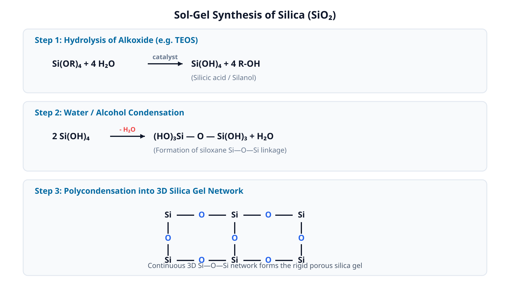
- Hydrolysis: Water attacks the metal or metalloid alkoxide precursor, replacing alkoxide groups () with hydroxyl groups () and liberating alcohol (). For silicon tetraalkoxide:
- Condensation and polycondensation: Hydrolysed species link together to form bridging oxygen bonds ( siloxane linkages), releasing either water (water condensation) or alcohol (alcohol condensation):
Continued three-dimensional polycondensation links oligomers into colloidal sol particles, which eventually interconnect across the vessel to form a rigid wet gel. Combining complete hydrolysis and condensation yields the overall stoichiometric summary for silica:
Similarly, titanium tetraisopropoxide () undergoes hydrolysis to followed by polycondensation, summarized overall as:
For alumina, aluminium alkoxide hydrolyses to aluminium hydroxide, which is subsequently dehydrated during thermal treatment:
-
Ageing and washing: The wet gel is kept in its pore liquid so unreacted groups continue condensing, strengthening the skeletal necking. Washing with fresh solvent removes soluble salt impurities and residual alcohol.
-
Drying: The method used to remove pore liquid dictates the final nanostructure:
- Evaporative drying Xerogel: Conventional thermal evaporation creates strong liquid–vapour capillary forces across tiny pores, causing the gel network to shrink and partially collapse into a dense xerogel.
- Supercritical drying Aerogel: Removing the pore fluid above its critical temperature and pressure inside an autoclave eliminates the liquid–vapour meniscus and capillary stress. This preserves the intact, highly porous solid skeleton as an ultra-low-density aerogel (for example, ethanol-exchanged silica gels are supercritically dried near the critical point of ethanol, around and , though exact parameters depend on the pore solvent used).
-
Calcination: Thermal treatment selected for the material can remove residual organic groups, promote dehydration, and, where required, crystallize an amorphous precursor (such as converting amorphous gel into crystalline anatase/rutile nano-).
Controlling particle size and preventing agglomeration
Across all bottom-up wet-chemical syntheses, final nanoparticle dimensions depend on the competition between nucleation (birth of new seeds) and growth (addition of material to existing seeds). Separating nucleation from growth can help narrow the size distribution, though the result depends on growth kinetics, ripening and aggregation.
Reaction temperature, precursor concentration, and solution govern these rates; for instance, acid-catalysed silica sol–gel favours weakly branched linear chains, whereas base catalysis produces compact spherical colloids. Because nanoparticles possess immense surface energy, bare particles spontaneously clump together (agglomeration) to minimize surface area. Steric polymers or electrostatic capping agents (like citrate) can be used during synthesis to create repulsive barriers that keep nanoparticles individually dispersed.
Example 1: Classifying nanoparticle synthesis routes
Problem: Classify each of the following processes as top-down or bottom-up, identify the primary chemical or physical mechanism, and state the chemical family of the final nanomaterial: (a) Planetary ball milling of graphite powder; (b) Heating aqueous with trisodium citrate; (c) Reacting with water followed by gelation and calcination at .
Solution:
-
(a) Planetary ball milling of graphite:
- Approach: Top-down.
- Mechanism: Mechanical attrition and shear fracture of bulk layered crystals into nanoscale platelets.
- Product family: Carbon nanomaterial.
-
(b) Reaction of with trisodium citrate:
- Approach: Bottom-up.
- Mechanism: Chemical reduction () accompanied by citrate electrostatic capping.
- Product family: Zero-valent metallic nanoparticles (nano-).
-
(c) Reaction of with water and calcination:
- Approach: Bottom-up.
- Mechanism: Sol–gel synthesis involving alkoxide hydrolysis, polycondensation ( network formation), drying, and thermal crystallization.
- Product family: Metal oxide nanoparticles (crystalline nano-).
Self-check questions
-
Question: Why does supercritical drying of a wet silica gel yield an aerogel with much higher porosity than conventional evaporative drying? Answer: Supercritical drying removes the pore fluid above its critical temperature and pressure, avoiding a liquid–vapour interface. This eliminates capillary surface-tension forces that otherwise pull pore walls together during conventional evaporation (which forms a shrunken xerogel).
-
Question: What two roles does trisodium citrate play during the synthesis of silver nanoparticles from silver nitrate? Answer: It acts as a chemical reducing agent (reducing ions to neutral atoms) and as an electrostatic capping agent (adsorbing onto nanoparticle surfaces to prevent agglomeration).
Graphene: structure, preparation, properties and uses
Structure and Bonding
Graphene
Graphene is a two-dimensional crystalline allotrope of carbon consisting of a single layer of carbon atoms arranged in a planar hexagonal honeycomb lattice. It serves as the structural building block for other graphitic nanomaterials, including fullerenes, carbon nanotubes, and bulk three-dimensional graphite.
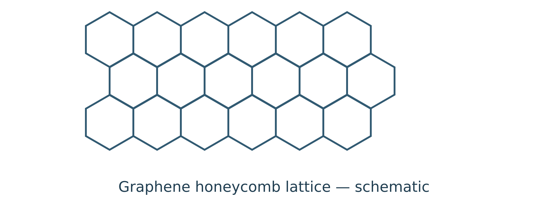
Figure 1: Two-dimensional hexagonal honeycomb lattice of monolayer graphene.
Every carbon atom in the graphene lattice is hybridized. Each atom forms three strong in-plane covalent bonds with its three nearest neighbours at bond angles of and a carbon–carbon bond length of . This rigid -bond framework gives the sheet exceptional mechanical stability.
The remaining fourth valence electron occupies an unhybridized orbital oriented perpendicular to the planar sheet. Lateral overlap of these out-of-plane orbitals across the lattice creates a delocalized electronic system consisting of a bonding valence band () and an antibonding conduction band ().
In ideal, neutral monolayer graphene at , the valence band is completely filled and the conduction band is completely empty. These two bands touch at six discrete points at the corners of the Brillouin zone, known as Dirac points. Because there is no energy gap between the valence and conduction bands at the Dirac points, graphene is classified as a zero-bandgap semiconductor or a semimetal. Charge transport can occur via either electrons or holes, with the dominant carrier type controlled by chemical doping or electrostatic gating.
Watch out. Student notes often state that the and orbitals form "two half-filled bands." Actually, the two-band system is half occupied overall, rather than both bands individually being half-filled; in neutral undoped graphene at absolute zero, the lower valence band is fully occupied and the upper conduction band is completely empty.
Preparation Methods
Different synthesis routes yield graphene with varying flake sizes, defect densities, and scalability:
- Mechanical exfoliation (Scotch-tape method): Repeatedly peeling bulk graphite using adhesive tape overcomes the weak van der Waals forces between stacked layers, leaving behind isolated single-layer graphene flakes. This yields pristine, low-defect crystals ideal for fundamental research, though the original adhesive-tape method has low throughput.
- Chemical vapour deposition (CVD): A carbon-containing precursor gas such as methane () is decomposed at high temperature over a catalytic transition-metal substrate (commonly copper or nickel). Carbon atoms dissolve into or adsorb onto the metal surface and reorganize into a continuous graphene film, which can then be transferred to insulating substrates.
- Thermal decomposition of silicon carbide (): Heating a single-crystal wafer to high temperatures under suitable vacuum or controlled-atmosphere conditions causes silicon atoms to sublime (evaporate) from the surface faster than carbon. The remaining surface carbon atoms rearrange into an epitaxial graphene layer directly on the wafer.
- Reduction of graphene oxide (GO): Graphite is chemically oxidized and exfoliated into water-dispersible graphene oxide sheets, which are then treated with chemical reducing agents or thermal annealing. This produces reduced graphene oxide (rGO), a scalable bulk material that retains structural defects and residual oxygen functional groups rather than yielding pristine graphene.
| Synthesis Method | Principle | Product Quality & Scalability |
|---|---|---|
| Mechanical exfoliation | Peeling graphite layers with adhesive tape | Highest crystal quality; very low yield |
| Chemical vapour deposition (CVD) | Pyrolysis of hydrocarbon gas on or | Large-area continuous films; moderate cost |
| Thermal decomposition of | Sublimation of leaves surface to graphitize | Wafer-scale epitaxial films; high substrate cost |
| Graphene oxide reduction | Chemical or thermal reduction of exfoliated GO | High bulk scalability; defective rGO sheets |
Key Properties
The properties of graphene depend strongly on sample purity, layer count, defect density, and substrate interactions:
- Mechanical strength: The short, rigid in-plane bonds give defect-free monolayer graphene an extraordinarily high intrinsic tensile strength and Young's modulus, while allowing the sheet to flex out of plane without breaking.
- Electrical and thermal transport: Delocalized electrons and low-mass charge carriers near the Dirac points provide remarkably high room-temperature carrier mobility and electrical conductivity. Strong covalent bonding also enables efficient phonon transport, resulting in high in-plane thermal conductivity.
- Optical transparency: Despite its dense atomic packing, a single monolayer of graphene absorbs only about of incident visible light, making it highly transparent.
- Specific surface area: Because graphene is a single atom thick, every carbon atom lies on the surface and is exposed on both sides of the sheet, resulting in a very high theoretical specific surface area ().
Applications
- Electronics and optoelectronics: High optical transparency and low sheet resistance make graphene films attractive as flexible transparent conductive electrodes for touchscreens, liquid-crystal displays, and organic solar cells. While high carrier mobility enables ultra-high-frequency analog and radio-frequency transistors, the absence of an energy bandgap prevents pristine graphene transistors from switching off completely, limiting its direct use in standard digital logic gates.
- Energy storage: Graphene and rGO are widely incorporated into electrodes for supercapacitors, lithium-ion batteries, and fuel cells. The high accessible surface area supports rapid ion adsorption in supercapacitors, while the conductive carbon network lowers internal resistance and improves charge/discharge rates in composite battery electrodes.
Watch out. Adding graphene to a battery electrode does not automatically increase its reversible storage capacity. Graphene primarily acts as a conductive, mechanically stable scaffold that accelerates electron transport and buffers volume changes during cycling.
- Composites and coatings: Well-dispersed graphene or rGO in suitable polymers, metals or coatings can improve mechanical stiffness, electrical conductivity, and barrier resistance against corrosive gases and moisture for aerospace and sporting goods.
- Environmental membranes and filtration: An ideal defect-free graphene sheet strongly blocks ordinary molecular permeation; defects and functionalization change this behaviour. However, engineering nanopores of controlled size into graphene sheets or stacking graphene oxide layers with defined interlayer channels produces selective membranes for water desalination, pollutant filtration, and gas separation.
- Biomedical research: Functionalized graphene derivatives are actively investigated for electrochemical biosensors and targeted drug-delivery carriers, where high surface area allows loading of aromatic chemotherapy molecules; clinical deployment requires careful control of flake size, surface chemistry, and long-term biocompatibility.
Self-Check Questions
- Why is pristine monolayer graphene unsuited for conventional digital logic switches despite its high carrier mobility? Answer: Pristine graphene is a zero-bandgap semimetal where the valence and conduction bands touch at the Dirac points. Without an energy bandgap, a graphene field-effect transistor cannot be completely switched "off," leading to high leakage currents.
- What happens during the thermal decomposition of to form graphene? Answer: When is heated under ultra-high vacuum, silicon atoms sublime from the surface, and the remaining carbon atoms reorganize into a hexagonal graphene lattice.
Fullerenes and the structure of C₆₀
Fullerenes
Fullerenes are discrete, zero-dimensional () hollow closed-cage molecules composed entirely of carbon atoms. Unlike diamond or graphite, which form extended three-dimensional or layered networks, fullerenes exist as individual molecular cages (, , , and higher homologues).
Buckminsterfullerene
Buckminsterfullerene (), often called a "buckyball" because its polyhedral cage resembles a standard soccer ball, is the most abundant and thoroughly studied member of the fullerene family.
Geometric Structure and Bonding in
The molecule adopts the geometry of a truncated icosahedron (not a regular icosahedron, which has only 12 vertices and 20 triangular faces). A truncated icosahedron has equivalent vertices, edges, and faces consisting of regular pentagons and hexagons. A carbon atom occupies each of the vertices.
Every carbon atom in is three-coordinate, bonded to three neighboring carbon atoms at the junction of one pentagon and two hexagons. In a flat graphene sheet, three-coordinate carbon is purely hybridized with bond angles. In a closed spherical cage, however, the pentagonal rings introduce curvature ( interior angles in a regular pentagon). This forces the carbon network to bend out of plane—a geometric distortion known as pyramidalization. Consequently, every carbon atom in exhibits a curved, -like hybridization with a slight character due to curvature, rather than the molecule containing a mixture of separate and carbon atoms.
Because of this cage topology, has two distinct types of covalent carbon–carbon bonds:
- bonds: Located at the fusion of two hexagonal rings ( such edges in ). These bonds are shorter (approx. ) and possess significant double-bond character.
- bonds: Located at the fusion of a pentagonal ring and a hexagonal ring ( such edges in ). These bonds are longer (approx. ) and possess mostly single-bond character.
The two edge environments produce different bond orders and lengths within the cage’s electronic structure. Therefore, does not have equal bond lengths throughout and is not uniformly delocalized like benzene.
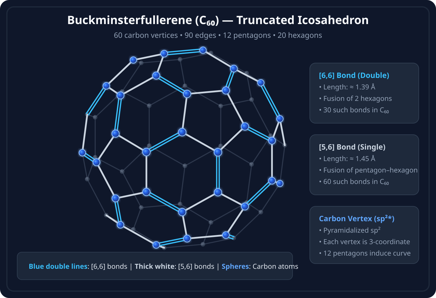
Figure: Truncated icosahedral structure of buckminsterfullerene () showing 12 pentagonal rings, 20 hexagonal rings, short double bonds, and long single bonds.
Watch out. Not all fullerenes contain 20 hexagons. By Euler's polyhedron theorem, any closed trivalent carbon cage built exclusively from pentagons and hexagons must contain exactly 12 pentagons, while the number of hexagons varies with molecular size (for example, has 12 pentagons and 25 hexagons, whereas has 12 pentagons and zero hexagons).
Example 1: Topological verification of the cage (Illustrative learning example)
Problem: Assuming is a closed convex polyhedron where every carbon vertex () is shared by exactly three edges and all faces are either pentagons () or hexagons (), calculate the total number of edges (), total faces (), pentagonal faces (), and hexagonal faces ().
Solution:
- Since each of the vertices connects to edges, and each edge connects vertices:
- Apply Euler's theorem for a closed convex polyhedron ():
- Express total faces and edges in terms of pentagons and hexagons (each shared edge belongs to faces):
- Substitute into the edge equation:
- Solve for :
Preparation of
Fullerenes are synthesized by high-temperature vaporization of graphite in an inert atmosphere:
- Vaporization: An electric arc is struck between high-purity graphite electrodes inside a chamber filled with low-pressure inert helium () gas.
- Condensation: The intense heat vaporizes carbon into reactive clusters that cool and condense in the helium buffer gas to form fullerene-rich soot (containing mostly , smaller amounts of , and higher fullerenes).
- Extraction: Fullerenes are separated from insoluble graphitic soot by solvent extraction using an organic solvent such as toluene or benzene.
- Purification: Pure is isolated from the extracted fullerene mixture by column chromatography on alumina or silica stationary phases.
Properties of
| Property Category | Key Characteristics |
|---|---|
| Physical state & Solubility | Dark crystalline powder at room temperature; sparingly soluble in aromatic solvents, forming a characteristic magenta/violet solution in benzene or toluene. |
| Mechanical behavior | Individual cages are resilient to compression, but bulk solid (fullerite) is a soft molecular solid held together by weak van der Waals forces. |
| Optical absorption | Absorbs strongly in the ultraviolet (UV) region and moderately across the visible spectrum due to electronic transitions. |
| Electrical & Redox behavior | Pristine solid is a poor electrical conductor (wide-gap semiconductor/insulator). However, the cage is a strong electron acceptor (accepting up to 6 electrons). Intercalating alkali metals into the lattice yields alkali-doped fullerides (, such as ), some of which become metallic and exhibit superconductivity at cryogenic temperatures. |
Watch out. Standard solid is not harder than diamond or steel. While an individual cage resists deformation, the bulk solid consists of discrete molecules bound by weak intermolecular forces and is easily sheared.
Applications
- Organic photovoltaics and electronics: Functionalized fullerene derivatives (such as PCBM) are widely used as electron-accepting materials in bulk-heterojunction organic solar cells and organic photodetectors.
- Lubricants and protective coatings: Because spherical molecules interact weakly with one another, they can act like molecular ball bearings in solid lubricant additives and wear-resistant surface coatings.
- Catalysis and chemical sensors: Fullerenes serve as electron-transfer mediators in heterogeneous catalysis and as active sensing layers for detecting volatile organic compounds or environmental pollutants.
- Biomedical research: Pristine is hydrophobic and poorly water-soluble. Chemically modified forms are a research topic: water-soluble fullerene derivatives and endohedral metallofullerenes (such as gadolinium-encapsulated cages, ) are investigated in research settings as radical-scavenging antioxidants, photosensitizers for photodynamic therapy, targeted drug-delivery carriers, and magnetic resonance imaging (MRI) contrast agents.
Self-Check Questions
- Why does exhibit two different carbon–carbon bond lengths instead of a single uniform bond length like benzene? Answer: In , bonds sit in two geometrically distinct environments: junctions between two hexagons and junctions between a pentagon and a hexagon. The edges have greater double-bond character and are shorter, while the edges are longer. This does not imply that all cage bonds have equal aromatic bond order.
- How does doping with potassium change the electrical behavior of solid ? Answer: Pristine solid is an electrical insulator/semiconductor with localized molecular orbitals, but potassium atoms transfer valence electrons into the conduction band to form the ionic fulleride salt , which conducts electricity and becomes superconducting at low temperatures.
Carbon nanotubes: structure, chirality and applications
Carbon nanotubes (CNTs)
Carbon nanotubes (CNTs) are one-dimensional cylindrical allotropes of -hybridized carbon. While their outer diameters lie in the nanoscale ( to ), their lengths can reach several micrometres or millimetres, creating exceptionally high aspect ratios. Structurally, a carbon nanotube is conceptualized as a single-atom-thick graphene sheet rolled into a seamless hollow cylinder. This rolling is strictly a geometric model used to describe bond orientation; in practice, CNTs are not manufactured by mechanically rolling flat graphene sheets.
Structural classification
Carbon nanotubes are categorized by the number of concentric graphitic walls present in the cylinder.
Single-walled carbon nanotubes (SWCNTs)
Single-walled carbon nanotubes consist of a single seamless graphene cylinder with typical diameters of to .
Multi-walled carbon nanotubes (MWCNTs)
Multi-walled carbon nanotubes consist of multiple nested graphene cylinders with outer diameters ranging from to and an interlayer spacing of approximately (close to that of graphite).
In structural descriptions, standard MWCNTs follow the Russian Doll model, where discrete concentric cylinders of increasing diameter are nested inside one another. Introductory texts often mention a Parchment (or scroll) model, in which a single graphene sheet is spirally wound around itself like a rolled scroll of paper, and a Mixed model combining both features. Strictly speaking, a spirally wound sheet is a distinct nanostructure called a carbon nanoscroll (which has open edges rather than closed seamless walls), though it is informally grouped with MWCNTs in basic classifications.
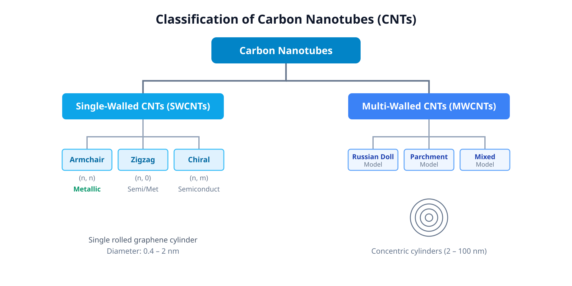
Figure: Classification tree of single-walled carbon nanotubes (SWCNTs: armchair, zigzag, chiral) and multi-walled carbon nanotubes (MWCNTs: Russian doll, parchment, mixed).
Chirality and electronic behaviour
The electronic properties of an SWCNT depend on the direction in which the conceptual graphene sheet is rolled, defined by the chiral vector ():
Here, and are the unit vectors of the hexagonal graphene lattice, and are non-negative integers (, with ) called chiral indices. The magnitude of sets the circumference of the nanotube.
| Geometry | Chiral Indices | Chiral Angle () | Cross-Sectional Edge Pattern | Electronic Character (Zone-Folding Rule) | Concrete Example |
|---|---|---|---|---|---|
| Armchair | Symmetrical armchair | Truly metallic (zero band gap) | — Metallic | ||
| Zigzag | Symmetrical zigzag | Metallic if is a multiple of ; otherwise semiconducting | — Semiconducting; — Quasi-metallic | ||
| Chiral | Helical twist | Metallic if is a multiple of ; otherwise semiconducting | — Quasi-metallic; — Semiconducting |
Confining electrons around the narrow circumference quantizes their allowed wavevectors. In the simple zone-folding approximation, an SWCNT is metallic whenever:
Watch out. Do not assume that all chiral nanotubes are semiconductors, or that every tube satisfying is an ideal metal. Only armchair nanotubes are metallic in the ideal unperturbed model because their symmetry prevents the usual curvature-induced gap. In non-armchair tubes where , the mechanical curvature of small-diameter walls slightly misaligns the -orbitals, opening a tiny secondary band gap and making them quasi-metallic (narrow-gap semiconductors).
Example 1: Classifying SWCNTs by Chiral Indices
Determine the geometric class and electronic character of , , and single-walled carbon nanotubes.
Solution:
- For : Since , this is an armchair nanotube. Applying the rule gives , which is divisible by . Because armchair symmetry prevents curvature-induced band gaps, the tube is truly metallic.
- For : Since , this is a zigzag nanotube. Here, , which is not divisible by . The tube is semiconducting.
- For : Since , this is a zigzag nanotube. Here, , which is a multiple of . It is nominally metallic by zone folding, though tube curvature opens a very small band gap (quasi-metallic).
Synthesis, properties and applications
CNTs are synthesized using three primary routes:
- Chemical Vapour Deposition (CVD): Catalytic decomposition of a hydrocarbon gas (such as methane, ethylene, or acetylene) over transition-metal catalyst nanoparticles (, , or ) at . CVD is the standard commercial method because it allows scalable growth and control over alignment.
- Arc Discharge: Vaporizing graphite electrodes via a high-current electric arc in an inert helium atmosphere.
- Laser Ablation: Vaporizing a metal-doped graphite target inside a high-temperature furnace using pulsed laser irradiation.
Anisotropic properties
Because strong covalent bonds run along the tube axis while only weak van der Waals forces act between adjacent tubes, CNT properties are highly anisotropic (direction-dependent).
- Mechanical: Individual defect-free CNTs exhibit high axial Young's modulus () and tensile strength () at low mass density (, roughly one-sixth to one-fourth that of steel). Bulk CNT fibres are weaker than ideal individual tubes because tubes slide past one another.
- Electrical and Thermal: Metallic SWCNTs support nearly ballistic axial electron transport and high axial thermal conductivity, whereas transport perpendicular to the tube axis is poor. Real device conductivity depends strongly on tube diameter, chirality, lattice defects, and metal contact resistance.
Watch out. Avoid unconditional claims that CNTs are "100 times stronger than steel" or "better conductors than all metals" in bulk form. Such comparisons depend on the specimen, reference material and measurement; bulk bundles and composites are limited by defects and tube-to-tube contact resistance.
Practical applications
- Structural Composites: Dispersed in polymers for lightweight aerospace, automotive, and sporting components, as well as antistatic and electromagnetic-shielding coatings.
- Energy and Electronics: Conductive additives in lithium-ion battery electrodes and supercapacitors, transparent conductive films, and field-effect transistor (FET) channels.
- Sensing and Microscopy: High-aspect-ratio cantilevers and probe tips in Atomic Force Microscopy (AFM) for high-resolution imaging of biomolecules such as DNA and proteins, as well as electrochemical gas and biosensors.
- Emerging Research: Investigated as high-surface-area adsorbents for gas/hydrogen storage, water purification membranes, and functionalised carriers for targeted drug delivery (requiring surface modification to control toxicity and biodistribution).
Self-Check Questions
- Why can ideal and nanotubes have different band-gap behaviour even though is divisible by for both? Answer: The tube has armchair symmetry (), which preserves a zero band gap in the ideal unperturbed model. The zigzag tube suffers from curvature-induced -orbital misalignment, which opens a small band gap.
- Why are the mechanical strength and electrical conductivity of carbon nanotubes much higher along the tube axis than perpendicular to it? Answer: Along the tube axis, atoms are linked by strong covalent bonds and continuous delocalized -electron networks, whereas adjacent tubes interact only through weak van der Waals forces.
Carbon quantum dots and applications of nanomaterials
Structure and optical emission
Carbon quantum dots (CQDs)
Carbon quantum dots (CQDs) are zero-dimensional, quasi-spherical carbon nanoparticles that are typically smaller than . Within the broader family of carbon dots, true CQDs usually possess a crystalline graphitic () core, whereas related carbon nanodots may have an amorphous or mixed carbon core. Surfaces often carry oxygen- or nitrogen-containing functional groups (such as , , and ), which impart water dispersibility and provide sites for chemical passivation.
Unlike conventional inorganic semiconductor quantum dots, not all carbon dots share a single light-emission mechanism. Depending on the synthesis route and surface passivation, emission can arise from quantum confinement in conjugated -domains, surface-defect trap states, or embedded molecular fluorophores.
CQDs absorb strongly in the ultraviolet (UV) region due to and electronic transitions, and emit tunable visible light.
Photoluminescence
Photoluminescence (including fluorescence) occurs when CQDs absorb external excitation light to produce emission.
Chemiluminescence
Chemiluminescence occurs under specific chemical redox reactions in certain functionalized CQDs, where the energy for light emission comes from a chemical reaction rather than absorbed photons.
Watch out. Do not assume that all carbon quantum dots emit purely by size-dependent quantum confinement or that they automatically glow without an excitation source. Photoluminescence requires light absorption, chemiluminescence requires a specific chemical reaction, and surface functional groups often dominate the emission wavelength.
Synthesis routes
CQDs are prepared by two general strategies:
- Top-down methods cleave larger carbon structures (such as graphite, carbon nanotubes, or activated carbon) into nanoscale fragments using electrochemical oxidation, laser ablation, or arc discharge.
- Bottom-up methods assemble CQDs from small organic precursors (such as citric acid, glucose, or urea) via hydrothermal treatment, microwave-assisted pyrolysis, or thermal carbonization.
Although CQDs avoid toxic heavy metals and often show good biocompatibility, they cannot be declared universally safe; toxicity and environmental impact must still be assessed for each specific surface chemistry and dosage.
Comparing nanoscale optical materials
Reducing particle size into the regime alters optical behavior, but the underlying physics depends on the material class.
| Material class | Typical example | Primary optical mechanism | Key chemical consideration |
|---|---|---|---|
| Semiconductor quantum dots | , | Size-dependent quantum confinement across a bandgap | High luminescence efficiency, but ions pose severe toxicity risks |
| Metal nanoparticles | Colloidal , | Localized surface plasmon resonance (collective electron oscillation) | Size and shape tune absorption color (e.g., ruby-red gold glass) |
| Carbon quantum dots | Surface-passivated CQDs | Combined core confinement, surface states, and molecular states | Heavy-metal-free and tunable, though quantum yield varies with passivation |
Watch out. Source notes often group gold () and cadmium selenide () nanoparticles together as colorants. Gold nanoparticles color glass via surface plasmon resonance, whereas and nanocrystals show size-tunable emission via quantum confinement and contain cadmium, requiring careful assessment of exposure and disposal.
Applications of nanomaterials
When bulk materials are reduced to the nanoscale, the fraction of atoms residing at the surface increases sharply. This high surface-to-volume ratio, combined with tunable electronic and mechanical traits, drives applications across several engineering sectors:
- Catalysis: Selected metal, metal-oxide or supported nanocatalysts provide accessible active sites. Their chemistry can lower the activation barrier for particular industrial or environmental reactions; high surface area alone does not make every nanoparticle a catalyst.
- Gas sensors: Nano-sized metal oxides provide large reactive surface areas where adsorbed gas molecules transfer charge, producing rapid, measurable changes in electrical resistance.
- Electronics and optoelectronics: Carbon nanotubes, fullerenes, and quantum dots enable component miniaturization, flexible circuits, high-resolution displays, light-emitting diodes (LEDs), paper batteries, and window or photoactive layers in solar cells.
- Coatings and structural reinforcement: Dispersing carbon nanomaterials (such as carbon black or nanotubes) into elastomers improves mechanical strength, wear resistance, and thermal conductivity in synthetic tyres.
- Environmental remediation: Suitable membranes and adsorbents separate or capture contaminants, while selected nanocatalysts can degrade some organic pollutants. Adsorption and degradation are different processes.
- Biomedicine: Functionalized nanoparticles and fluorescent dots are investigated for bioimaging, sensing and delivery. Suitability depends on the formulation and biological evidence; it cannot be assumed from nanoscale size alone.
In every application, performance depends on maintaining uniform nanoparticle dispersion; agglomeration reduces active surface area and degrades optical or mechanical properties.
Self-check questions
- Why do gold nanoparticles and quantum dots produce size-dependent colors through different physical mechanisms? Answer: Gold nanoparticles are metallic and absorb specific wavelengths via localized surface plasmon resonance, whereas is a semiconductor whose bandgap energy shifts with crystal size due to quantum confinement.
- How does a high surface-to-volume ratio improve both heterogeneous catalysis and gas sensing? Answer: It exposes a much larger fraction of reactive surface atoms per unit mass, providing more active sites for catalytic bond breaking and more adsorption sites for gas molecules to alter electrical conductivity.
Polymer fundamentals and flame retardancy
Polymers
Polymers are macromolecules of high molecular mass built by covalently linking numerous small reactive molecules called monomers.
Repeat unit
A repeat unit is the structural unit enclosed in brackets that repeats along the chain. The number of repeat units is the degree of polymerization.
Depending on monomer identity and polymerization mechanism, polymers are classified into distinct structural and kinetic groups.
| Classification Basis | Category | Definition | Common Examples |
|---|---|---|---|
| Monomer Identity | Homopolymer | Derived from a single monomer species with one repeating unit. | Polyethylene (PE, ), Polyvinyl chloride (PVC, ) |
| Monomer Identity | Copolymer | Synthesized from two or more distinct monomers linked in the same chain. | Styrene–butadiene rubber (SBR), Acrylonitrile–butadiene–styrene (ABS) |
| Growth Mechanism | Addition (Chain-Growth) | Monomers add sequentially to an active site without losing atoms; repeat mass equals monomer mass. | Polyethylene, PVC, Polystyrene () |
| Growth Mechanism | Condensation (Step-Growth) | Multifunctional monomers react stepwise, typically eliminating a small molecule like or . | Nylon 6,6, Bakelite (note: some step-growth polymers like polyurethanes form without eliminating a small molecule) |
Flame-retardant polymer systems
Most commodity hydrocarbon polymers—such as polyethylene, polypropylene (), and polystyrene—pyrolyze easily into volatile fuels and burn rapidly.
Flame-retardant polymer systems are engineered to resist ignition, slow flame spread, and reduce heat release rates in electronics, aerospace, and construction. No organic polymer is completely "fireproof" under extreme heat, and flame resistance does not automatically guarantee low or non-toxic smoke.
Watch out. Do not confuse inherently flame-retardant polymers with flame-retardant additives. Inherently resistant polymers have thermally stable backbones or covalently bound halogens, whereas additives are separate inorganic fillers or small organic molecules blended into flammable host resins.
Physical and condensed-phase mechanisms
Flame retardants interrupt the combustion cycle in the condensed (solid) phase or gas phase through three primary physical and chemical pathways:
-
Protective char and mass/heat barrier: Aromatic and heterocyclic polymers crosslink during pyrolysis to form a rigid carbonaceous char layer. This insulating barrier blocks oxygen diffusion to the underlying fuel and slows the escape of flammable pyrolysis gases.
-
Endothermic cooling and dilution: Inorganic hydroxide fillers, most notably aluminium hydroxide (alumina trihydrate, ATH), decompose endothermically when heated:
Here denotes thermal energy absorbed from the polymer matrix. This endothermic reaction absorbs heat and can delay further heating and pyrolysis, leaves a protective ceramic ash, and releases water vapour that dilutes combustible gases and oxygen in the flame zone.
- Intumescence: Phosphorus–nitrogen additives (such as ammonium polyphosphate combined with nitrogen-rich char formers) decompose to generate phosphoric acid derivatives that catalyse charring while releasing non-flammable gases (, ). The softening char swells into a thick, multicellular intumescent foam that insulates the underlying polymer.
Non-halogenated polymers
Non-halogenated systems rely on high bond dissociation energies, rigid aromatic rings, or inorganic backbones rather than halogen radical chemistry. While individual formulations must still pass specific fire certifications, several polymer classes exhibit strong intrinsic thermal resistance:
Phenolic resins
Acid-catalysed condensation of phenol with formaldehyde yields novolac, a linear thermoplastic prepolymer. Heating novolac with a crosslinking agent (such as hexamethylenetetramine) cures it into Bakelite, an infusible, three-dimensional thermoset network whose dense aromatic structure yields high char upon heating.
Aromatic heterocyclic polymers
Polyimides and polybenzoxazoles (PBO) possess rigid, resonance-stabilized ring systems along their main chains. They resist thermal cleavage up to very high temperatures and can form protective carbonaceous char under suitable decomposition conditions.
Silicones (polysiloxanes)
Built on an inorganic backbone, silicones oxidize in a fire to form a non-combustible, thermally insulating silica () ash layer on the surface.
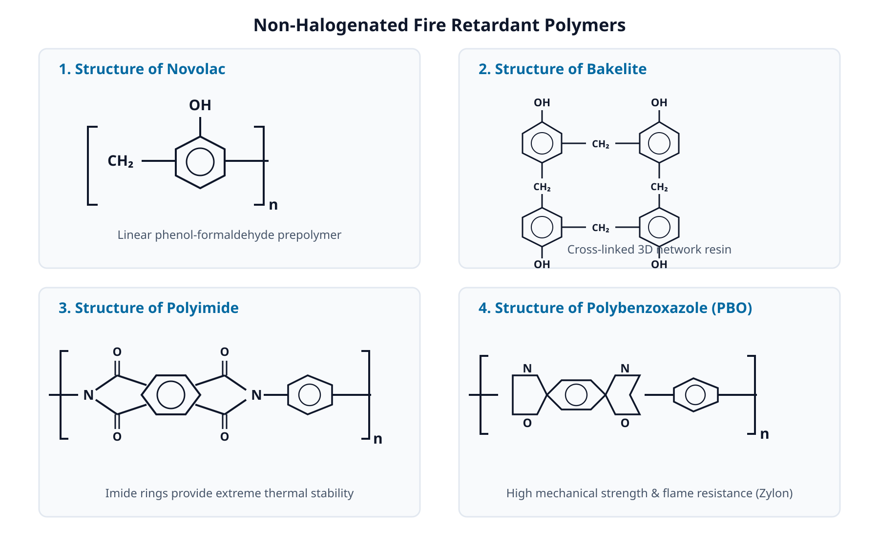
Figure 1: Idealized schematic repeat units and structural motifs of representative non-halogenated polymers (curing networks and copolymer ratios are simplified).
Halogenated polymers and gas-phase scavenging
Halogenated systems incorporate chlorine or bromine either covalently along the polymer backbone—as in polyvinyl chloride (PVC), neoprene (polychloroprene), and poly(bromostyrene)—or as blended small-molecule additives such as polybrominated diphenyl ethers (PBDEs) and polychlorinated diphenyl ethers (PCDEs). Note that brominated butyl rubber contains only a small mole fraction of bromine introduced primarily to promote vulcanization (curing) rather than to make the bulk elastomer inherently self-extinguishing.
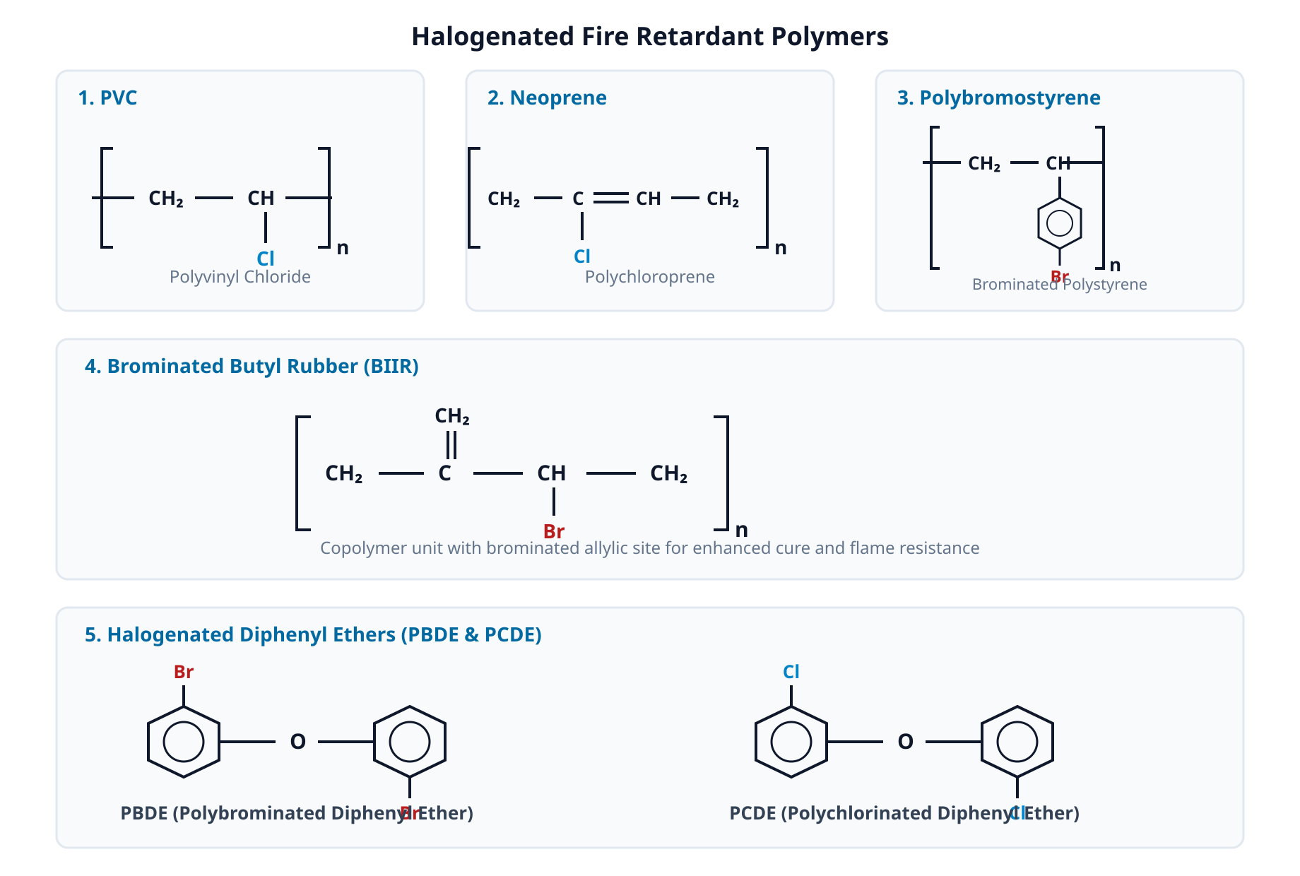
Figure 2: Representative halogenated polymers (PVC, Neoprene, Polybromostyrene, BIIR) and flame-retardant ether additives (PBDE, PCDE).
Loading molecular viewer...
Loading molecular viewer...
Watch out. Hydrocarbon flames propagate via high-energy chain-branching radicals ( and ). Halogenated polymers do not simply recombine or with to form stable or ; instead, they release hydrogen halides (, where or ) that catalyse radical scavenging in the gas phase.
During combustion, thermal decomposition and dehydrohalogenation can release hydrogen halides () into the flame zone:
- Radical scavenging: Hydrogen halide reacts with the highly reactive chain-propagating radicals and , replacing them with much less reactive halogen radicals (with bromine being markedly more effective than chlorine due to weaker and bonds):
- Hydrogen halide regeneration: The low-energy radical abstracts a hydrogen atom from a gaseous fuel molecule (), regenerating to continue the inhibition cycle:
Although elementary radical recombination steps (not shown) are required to achieve net radical termination, replacing energetic and carriers with sluggish radicals sharply reduces the rate of exothermic chain branching and quenches the flame. However, incomplete combustion and evolution often increase dark smoke and produce corrosive, toxic acidic fumes (, ), creating an engineering trade-off between ignition resistance and smoke hazard.
Example 1: Classifying Flame-Retardant Mechanisms in Electronic Enclosures
Problem: An electronics manufacturer evaluates three materials for circuit-board housings: (a) cured phenolic resin (Bakelite), (b) polypropylene filled with , and (c) poly(bromostyrene). Identify the primary phase of action (condensed vs gas phase) and the dominant flame-retardant mechanism for each.
Solution:
- Cured phenolic resin (Bakelite): Acts in the condensed phase. Its dense aromatic network crosslinks upon heating to form an insulating carbonaceous char barrier that blocks oxygen ingress and heat transfer.
- Polypropylene with (ATH): Acts in both the condensed and gas phases. ATH decomposes endothermically (), cooling the solid polymer, forming a ceramic barrier, and releasing water vapour to dilute flame gases.
- Poly(bromostyrene): Acts primarily in the gas phase. Pyrolysis releases , which scavenges high-energy and flame radicals and replaces them with less reactive radicals.
Self-Check Questions
- Question: Why does neat polyethylene being non-halogenated not make it inherently flame retardant? Answer: Polyethylene () lacks halogen atoms, but its aliphatic and bonds cleave readily upon heating into volatile, flammable hydrocarbon fragments without forming protective char.
- Question: How does novolac differ structurally from Bakelite, and why is curing required for high-temperature electronic applications? Answer: Novolac is a linear, fusible thermoplastic prepolymer that softens when heated, whereas curing crosslinks novolac chains into Bakelite—a rigid, infusible 3D thermoset network that retains structural integrity and chars rather than melting in a fire.
Conducting polymers: conjugation, doping and composites
Conjugated Backbones and Electronic Structure
Conventional organic polymers such as polyethylene contain only saturated bonds with tightly localized electrons, making them electrical insulators.
Intrinsically conducting polymers
Intrinsically conducting polymers (such as polyacetylene, polypyrrole, and polyaniline) possess an extended conjugated backbone of alternating single and double bonds, such as in polyacetylene.
Each -hybridized carbon atom along this backbone contributes an unhybridized orbital perpendicular to the chain axis. Continuous lateral overlap of these orbitals delocalizes electrons along the polymer segment, creating a filled valence band (-bonding orbitals) and an empty conduction band (-antibonding orbitals).
Loading molecular viewer...
Watch out. The band gap () separating the valence and conduction bands is an energy difference measured in electron-volts (), not a physical spatial distance. Furthermore, conjugation alone does not make a polymer metallic: because of bond-length alternation (Peierls distortion), undoped conjugated polymers typically have significant band gaps () and behave as low-conductivity semiconductors or insulators at room temperature.
Doping and Charge Transport
Doping in conducting polymers
Doping introduces mobile charge carriers along the conjugated polymer backbone, balanced by counter-ions to maintain overall electrical neutrality. Unlike conventional substitutional doping of inorganic semiconductors, polymer doping fundamentally proceeds through redox reactions or acid–base protonation.
p-Type (oxidative) doping
An oxidizing agent removes electrons from the polymer valence band, generating positively charged carriers on the chain () balanced by dopant counter-anions ():
Common oxidative dopants include iodine () and iron(III) chloride (). Although and are Lewis acids, p-doping fundamentally requires electron oxidation; not every Lewis acid can oxidize a polymer backbone unless a suitable oxidizing pathway is present.
n-Type (reductive) doping
A strong reducing agent (electron donor) such as sodium naphthalenide () injects electrons into the conduction band, creating negatively charged chains () balanced by counter-cations ():
Describing sodium naphthalenide merely as a Lewis base is imprecise; it functions here as a one-electron reducing agent.
Acid–base (protonic) doping
In heteroaromatic polymers with basic nitrogen sites, such as polyaniline (PANI), treating the half-oxidized emeraldine base with a protic acid (e.g., ) protonates the imine nitrogens. This increases conductivity by orders of magnitude without changing the average oxidation state of the polymer chain.
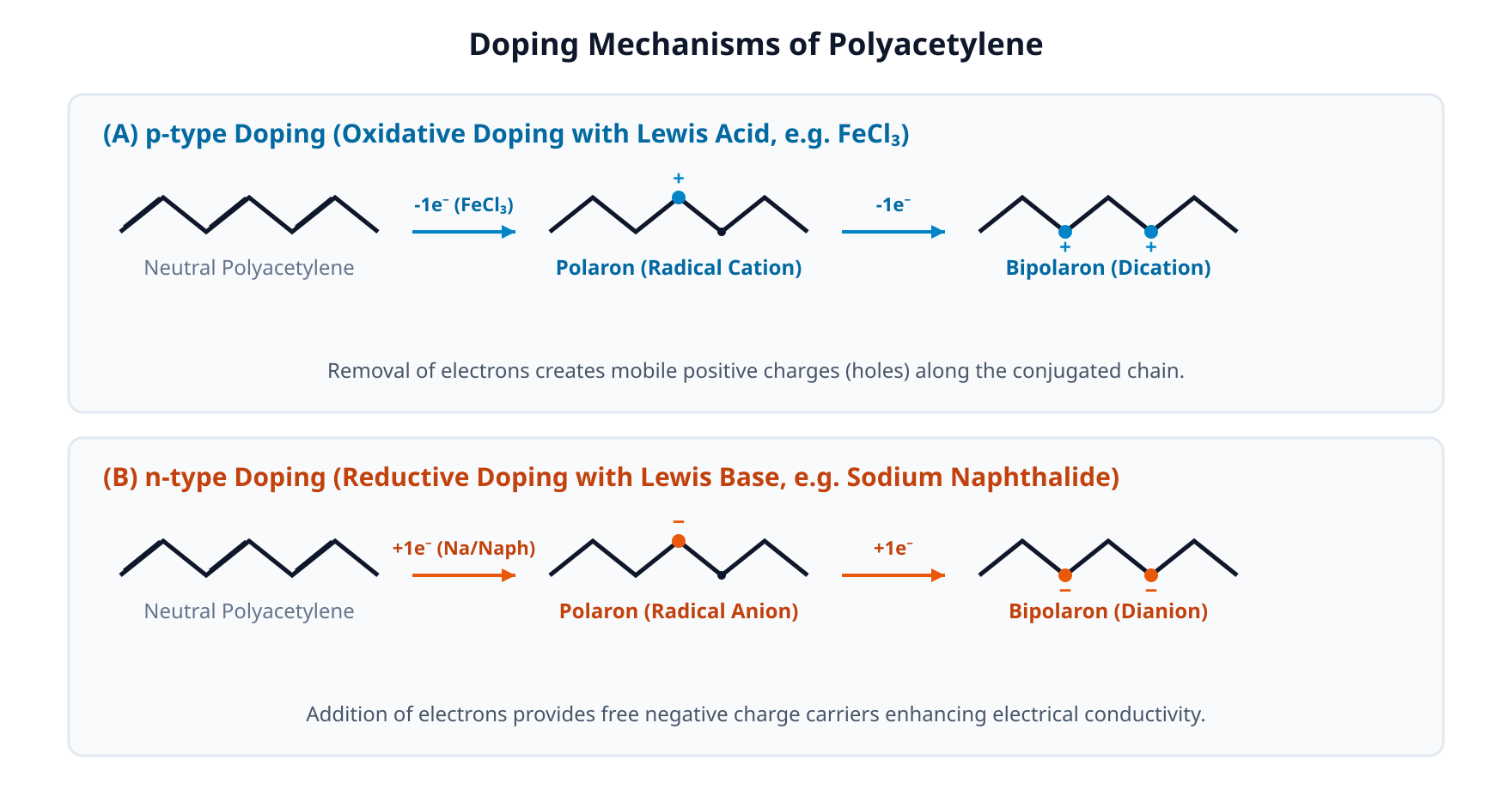
Figure: Simplified schematic of p-type oxidative doping and n-type reductive doping on a polyacetylene segment. Note that required counter-anions (for p-doping) and counter-cations (for n-doping) are omitted from this backbone view.
Charge carriers
When charge is added to or removed from a polymer chain, the surrounding bond lengths locally relax around the charge. Depending on backbone symmetry, these charge-coupled lattice deformations form quasi-particles:
- Polarons: Radical ions carrying spin and charge .
- Bipolarons: Spinless dications or dianions carrying charge .
- Solitons: Neutral radicals or spinless charged domain walls found in degenerate ground-state polymers such as trans-polyacetylene.
Macroscopic current requires two distinct transport steps:
- Intrachain transport: Rapid movement of polarons, bipolarons, or solitons along an individual conjugated chain via -bond rearrangement.
- Interchain hopping: Slower thermally activated hopping or tunneling of carriers between adjacent chains. Because interchain hopping usually limits overall conductivity, chain alignment, crystallinity, and film morphology strongly govern bulk performance.
Classification: Intrinsic vs Extrinsic Systems
Conducting polymer materials are grouped by whether the polymer chain itself carries the current or hosts an external conductor.
| Category | Subtype | Conduction Mechanism | Key Characteristics & Trade-offs |
|---|---|---|---|
| Intrinsically Conducting Polymers (ICPs) | Undoped conjugated polymers | Thermal or photo-excitation across | Low dark conductivity ( to ); useful as semiconducting layers in OLEDs and solar cells. |
| Intrinsically Conducting Polymers (ICPs) | Doped conjugated polymers (p-type, n-type, or protonated) | Intrachain delocalization + interchain hopping of polarons/bipolarons/solitons | High electronic conductivity ( to ); often stiffer and harder to melt-process than commodity plastics. |
| Extrinsically Conducting Polymers | Conductive-element-filled composites | Percolation across a touching network of carbon black, metal fibers, or silver powder inside an insulating binder (e.g., PVC) | Low cost, moldable, and mechanically tough, but conductivity drops sharply below the percolation threshold filler loading. |
| Extrinsically Conducting Polymers | Blended conducting polymers | Conducting domains of an ICP (e.g., polypyrrole) dispersed within a conventional matrix polymer (e.g., PVC or polystyrene) | Combines electrical conductivity with the host polymer's processability; phase separation and mechanical trade-offs must be carefully tuned. |
Applications
- Antistatic coatings and EMI shielding: Doped ICP blends and carbon- or metal-filled composites dissipate static charge and attenuate electromagnetic interference (EMI) in electronic housings.
- Electrochromic devices and OLEDs: Voltage-driven doping/dedoping switches the optical absorption of conducting polymers for smart windows, while undoped or doped layers serve as charge-transport or emissive layers in organic light-emitting diodes.
- Chemical and biosensors: Reversible conductivity or color changes upon exposure to gases (, ), shifts, or enzyme redox reactions (e.g., glucose oxidase) enable selective analytical sensors.
- Energy storage electrodes: Redox-active polymers such as polyaniline and polypyrrole act as pseudocapacitive or cathode-active materials in supercapacitors and rechargeable batteries.
Watch out. Do not confuse electronically conducting polymers (which transport electrons/holes along conjugated chains and serve as electrodes) with solid polymer electrolytes (such as -salt-doped poly(ethylene oxide), which transport ions and must be electronically insulating to prevent short-circuiting a battery).
Example 1: Identifying Dopant Roles and Polymer Charge States
Additional illustrative example. Suppose a neutral polypyrrole film () is oxidatively doped using iron(III) chloride () such that on average one electron is removed per four pyrrole monomer units, with incorporated as the counter-ion. Write the balanced oxidation half-reaction for a four-ring segment and identify the carrier type and counter-ion.
Solution:
- Oxidation of the polymer segment: Removing one electron from a four-unit segment creates a radical cation (positive polaron) on the backbone:
- Counter-ion balance: In doping, . The resulting doped polymer formula per four-ring segment is .
- Classification: Because electrons are removed from the system, this is p-type doping; the polymer backbone carries a positive charge, balanced by the negative counter-anion.
Self-Check Questions
- Question: Why does blending an intrinsically conducting polymer like polypyrrole with a conventional plastic like PVC not automatically guarantee superior mechanical and electrical properties at all ratios? Answer: Electrical conduction requires a continuous, percolating pathway of the conducting phase, whereas mechanical toughness relies on the host matrix and interfacial adhesion; poor phase compatibility or low conducting-polymer fraction can disrupt conduction or embrittle the blend.
- Question: How does acid doping of emeraldine-base polyaniline with differ chemically from doping of polyacetylene? Answer: oxidizes polyacetylene by removing electrons (changing the backbone oxidation state), whereas protonates the imine nitrogen sites of polyaniline without changing the mean oxidation state of the chain.
Polyaniline and polypyrrole: preparation, states and uses
Polyaniline (PANI) and polypyrrole (PPy) are two of the most widely studied intrinsically conducting polymers because their monomers are inexpensive, polymerization proceeds under mild aqueous or organic conditions, and their oxidized forms show good environmental stability. Unlike simple polyenes such as polyacetylene, both PANI and PPy contain heteroatoms () in or along the conjugated backbone, allowing electronic properties to be tuned through oxidation state and counterion incorporation.
Polyaniline: preparation and oxidation states
Polyaniline is synthesized by the oxidative polymerization of aniline () in an acidic medium, where aniline exists largely as the anilinium cation ().
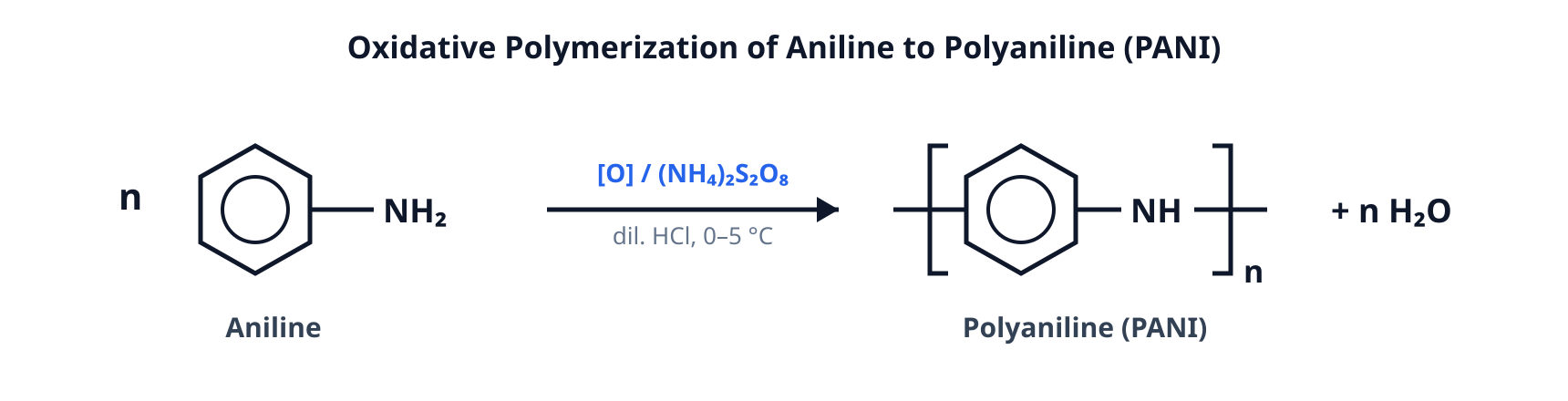
Figure: Preparation of polyaniline via oxidative polymerization of aniline monomers and conversion between emeraldine salt and base.
Loading molecular viewer...
Loading molecular viewer...
Chemical oxidative polymerization
- Dissolve aniline monomer in an aqueous acid such as dilute () and cool the solution in an ice bath ().
- Slowly add an aqueous solution of an oxidizing agent, typically ammonium persulfate (, APS), with continuous stirring. Low temperature is maintained because the oxidation is exothermic; cooling slows side reactions, limits chain branching or degradation, and yields a more regular head-to-tail (para-coupled) polymer.
- Under suitable reaction conditions, a dark green precipitate of protonated polyaniline (emeraldine salt) forms. It is collected by filtration and washed. Washing with dilute acid preserves the conductive salt, whereas washing with aqueous ammonium hydroxide () deprotonates the product to the blue emeraldine base.
Electrochemical polymerization
- Immerse an inert working electrode (such as platinum foil or conductive glass) and a counter electrode into an acidified aqueous solution of aniline.
- Apply a suitable anodic potential (specified relative to a named reference electrode and selected for the electrolyte and film-growth conditions) to oxidize the monomer at the anode surface.
- Radical cations couple directly on the positive electrode, depositing a uniform, adherent thin film of conducting polyaniline.
Watch out. Do not write a simplified polymerization equation releasing or unless the specific oxidant is balanced, because oxygen does not come from aniline. Also, never write " current"; voltage () is electric potential, whereas current is measured in amperes (), and the exact onset potential depends on the reference electrode and electrolyte.
Oxidation and protonation states of PANI
Polyaniline has a general repeat unit consisting of reduced benzenoid diamine units and oxidized quinonoid diimine units. Depending on the ratio of these units, PANI exists in three distinct oxidation states:
| Form of Polyaniline | Oxidation / Protonation State | Backbone Structure | Typical Colour | Electrical Behavior |
|---|---|---|---|---|
| Leucoemeraldine | Fully reduced | All benzenoid amine () units | Pale yellow / colourless | Insulator |
| Emeraldine base (EB) | Half-oxidized, unprotonated | benzenoid amine and quinonoid imine () | Blue | Poor conductor / semiconductor |
| Emeraldine salt (ES) | Half-oxidized, acid-protonated | Radical-cation (polaron) lattice with counterions () | Dark green | Highly conducting |
| Pernigraniline | Fully oxidized | Fully oxidized limiting form in the conventional PANI redox series, rich in quinonoid imine structure | Blue-violet | Insulator |
Crucially, the half-oxidized emeraldine form is not automatically conductive. Emeraldine base (EB) is an insulator or poor semiconductor until treated with a protonic acid (such as ), which protonates the imine nitrogens () without changing the number of electrons on the chain. This acid–base doping converts EB into the green emeraldine salt (ES), delocalizing polarons along the backbone and increasing conductivity by many orders of magnitude.
Polypyrrole: preparation and properties
Polypyrrole is formed by the oxidative polymerization of pyrrole (), a five-membered heteroaromatic ring containing an group. Monomer oxidation generates radical cations that couple predominantly at the -positions (carbon positions and adjacent to nitrogen), followed by deprotonation.
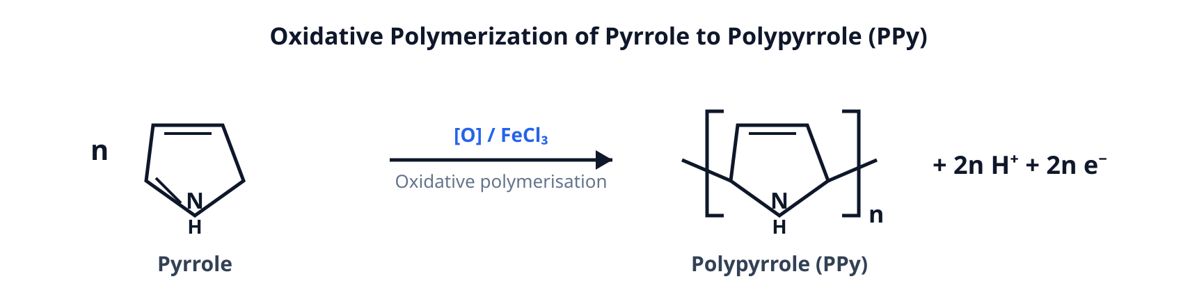
Figure: Oxidative polymerization of pyrrole to polypyrrole through 2,5-radical cation coupling.
Loading molecular viewer...
Loading molecular viewer...
Because the polymer has a lower oxidation potential than the monomer, the growing PPy chain is simultaneously oxidized (-doped) during synthesis, incorporating anions from the solution to maintain charge neutrality.
- Chemical method: Mixing an aqueous solution of pyrrole (e.g., ) with an oxidant such as ferric chloride () or ammonium persulfate () at room temperature or under cooling yields a black precipitate of oxidized, doped polypyrrole over several hours, which is filtered, washed, and dried.
- Electrochemical method: Electrolysis of pyrrole (e.g., ) in an aqueous or organic solvent such as acetonitrile containing a supporting electrolyte—for example, tetraethylammonium tetrafluoroborate (, )—using platinum electrodes deposits a blue-black doped PPy film directly on the anode.
Properties and practical limitations
- Electrical transport: Doped PANI (emeraldine salt) and doped PPy achieve high semiconductor-to-metallic conductivities (), though they remain less conductive than bulk metals such as copper (). In many semiconducting regimes, their electrical resistance decreases as temperature increases because charge transport occurs via thermally activated hopping between chains.
- Electrochromism: Both polymers change colour reversibly upon redox switching. Neutral (undoped) PPy thin films are yellowish-green, whereas oxidized (doped) PPy is blue-black; PANI switches between yellow, green, and blue/violet.
- Processability and stability: Both polymers have rigid conjugated backbones with strong interchain interactions, making them infusible and poorly soluble in common solvents (doped PPy is often brittle and intractable). While air-stable in their conducting states, exposing PPy or PANI to excessive anodic potentials causes irreversible overoxidation and loss of conductivity.
Applications of PANI and PPy
- Energy storage: Active electrode materials and conductive binders in rechargeable batteries and supercapacitors.
- Sensors and biosensors: Chemiresistive gas sensors (, , pH) and enzyme-immobilized biosensors (such as glucose oxidase on PPy or PANI films).
- Antistatic and EMI shielding: Coatings and polymer blends to dissipate static charge and shield electronic circuits from electromagnetic interference (EMI).
- Optoelectronics and coatings: Hole-injection/transport layers in OLEDs, counter electrodes in dye-sensitized solar cells, electrochromic smart windows, and corrosion-inhibiting coatings on metals.
Example 1: Classifying redox versus acid–base steps in PANI synthesis
Problem: During the synthesis and processing of polyaniline, three chemical steps are performed: (a) converting aniline monomer into an emeraldine salt precipitate using in , (b) washing that green precipitate with aqueous to obtain blue emeraldine base, and (c) treating the emeraldine base with aqueous to restore conductivity. Classify each step as a redox reaction or a non-redox acid–base reaction, and state which product is electrically conducting.
Solution:
- Step (a) is a redox reaction: Ammonium persulfate oxidizes aniline monomers (removing electrons and protons) to build the half-oxidized polyaniline backbone, while keeps it protonated as the conducting emeraldine salt.
- Step (b) is a non-redox acid–base deprotonation: deprotonates nitrogen sites and releases associated chloride counterions without changing the oxidation state of the polymer, yielding insulating emeraldine base.
- Step (c) is a non-redox acid–base protonation (protonic acid doping): protonates the imine nitrogens of emeraldine base without electron transfer, regenerating the emeraldine salt, which is the electrically conducting form.
Self-check questions
- Why is chemical polymerization of aniline carried out at rather than at boiling temperature? Answer: Monomer oxidation is exothermic; keeping the reaction at controls the reaction rate, suppresses unwanted side reactions and overoxidation, and promotes regular para-coupled chains with higher conductivity.
- Does polypyrrole synthesized by oxidative polymerization with require a separate post-synthesis doping step to become conductive? Answer: No. The growing polypyrrole chain has a lower oxidation potential than pyrrole monomer, so it is oxidized (-doped) in situ during polymerization and incorporates counter-anions from the reaction medium; their identity depends on the electrolyte and synthesis conditions.
OLEDs: layers, charge injection and light emission
Organic Light-Emitting Diode (OLED)
An Organic Light-Emitting Diode (OLED) is a solid-state optoelectronic device in which thin films of organic semiconductors emit light when an electric current passes through them. OLEDs do not require a separate light source or added mobile ions to operate.
Electroluminescence
Electroluminescence is the emission of light by a material in response to an electric current passing through it.
OLEDs are divided into two main families based on their active materials:
- Small-molecule OLEDs
- Polymer LEDs (PLEDs) that use conjugated polymers.
Device Construction and Layer Stack
An OLED consists of ultra-thin organic layers sandwiched between two electrodes on a supporting base. At least one electrode must be transparent so generated photons can escape.
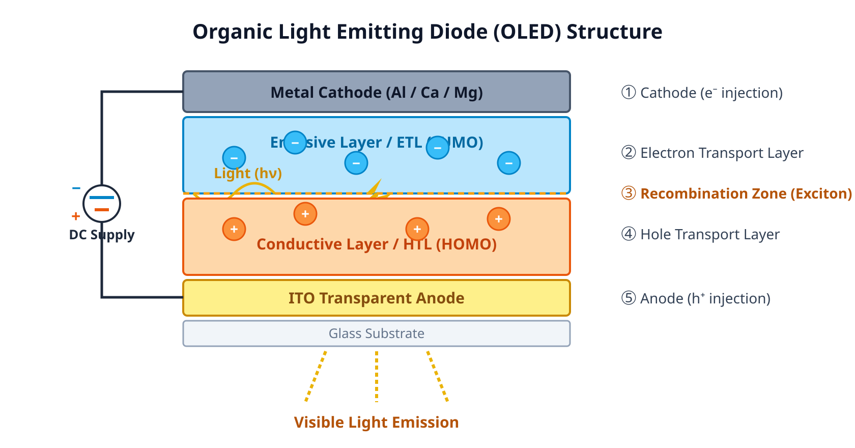
Figure: Simplified OLED architecture showing charge injection from electrodes and radiative recombination at the organic interface.
| Component | Typical Material | Primary Function |
|---|---|---|
| Substrate | Glass or flexible plastic foil | Provides mechanical support and optical transparency. |
| Anode | Indium tin oxide () | Transparent electrode that injects positive holes when forward biased. |
| Hole Transport Layer (HTL) | Polyaniline () or | Facilitates hole injection from the anode and transports holes toward the emitter. |
| Emissive Layer (EML) | Poly(p-phenylene vinylene) () or polyfluorene | Hosts electron–hole capture and radiative decay; simplified two-layer diagrams often combine the EML and Electron Transport Layer (ETL). |
| Cathode | Low-work-function metals/alloys (, , ) | Injects electrons into the adjacent organic layer and often acts as a reflective mirror. |
| Encapsulation | Glass lid or barrier film | Seals the stack against atmospheric oxygen and moisture. |
Watch out. Do not equate a physical device layer with a single molecular orbital (such as calling the EML the "LUMO layer" or the HTL the "HOMO layer"). Every organic molecule possesses both a Highest Occupied Molecular Orbital (HOMO) and a Lowest Unoccupied Molecular Orbital (LUMO). Electrons travel by hopping between LUMO states, whereas holes travel by hopping between HOMO states.
Charge Injection, Transport, and Light Emission
Light generation in an OLED occurs through a four-step microscopic sequence:
- Forward Bias and Charge Injection: A direct-current (DC) voltage is applied with the anode positive and the metallic cathode negative. The cathode injects electrons into the LUMO levels of the electron-transporting/emissive layer, while the anode removes electrons from the HOMO levels of the HTL, creating positive holes.
- Charge Migration: Under the applied electric field, electrons hop from molecule to molecule toward the anode, and holes hop in the opposite direction toward the cathode. Although holes have higher mobility than electrons in many common organic semiconductors, relative carrier speeds depend on the specific materials chosen; balanced transport is engineered so carriers meet inside the emissive zone.
- Exciton Formation: When an electron and a hole encounter each other on an emissive molecule, mutual Coulombic attraction binds them into a neutral, energetic electron–hole pair called an exciton.
- Radiative Recombination: The excited electron relaxes from the LUMO back down to the HOMO, annihilating the hole. If this transition is radiative, the released energy is emitted as a discrete photon of light. Non-radiative decay pathways (vibrational heat loss) compete with photon emission and reduce device efficiency.
Watch out. Moving an electron from the HOMO to the LUMO is excitation (energy absorption). Light emission occurs during the reverse transition, when an electron drops from the LUMO back to the HOMO. Furthermore, each recombination event releases a tiny quantum of energy (), not an "enormous" burst; continuous brightness comes from billions of recombinations occurring every second.
The emitted photon energy (in ) and wavelength (in ) are governed by the energy of the relaxing exciton:
Here is Planck's constant, is frequency, and is the speed of light; use wavelength in metres with in metres per second. Exciton binding, molecular relaxation and the solid-state environment affect the emitted energy, so it cannot be inferred exactly from a bare HOMO–LUMO gap. Synthetic chemists tune display colours—such as green from or blue from polyfluorene—by modifying polymer conjugation length and side groups to adjust this gap.
Example 1: Photon Energy of a Green Polymer OLED (Illustrative)
Calculate the energy in joules and electron-volts of a single photon emitted by a poly(p-phenylene vinylene) () OLED operating at a peak wavelength of . Assumptions: Assume a single photon is emitted radiatively at the peak wavelength; this calculation determines individual photon energy and makes no claim about overall device quantum efficiency. Constants: , , .
Solution: Convert the emission wavelength to metres:
Calculate the photon energy in joules:
Convert the photon energy to electron-volts:
Each emitted green photon carries () of energy.
Display Characteristics, Limitations, and Applications
Because every OLED pixel is self-emissive, no backlight or liquid-crystal shutter is needed. Turning a pixel's current off produces a true black state, yielding very high contrast ratios in dark environments, wide viewing angles (approaching off-axis), and microsecond response times. Depositing the thin stack onto plastic films rather than rigid glass enables lightweight, bendable, or foldable displays. Power consumption depends on image content: OLEDs use less power than backlit LCDs when showing dark interfaces, but can draw more power when displaying full-screen bright white content.
However, conjugated organic molecules are chemically vulnerable. Water vapour and oxygen rapidly oxidize the low-work-function cathode and degrade conjugated backbones, causing non-emissive "dark spots". Furthermore, blue emitters require a wide energy gap (), and these high-energy excitons accelerate bond cleavage, giving blue sub-pixels a shorter operational lifetime than red or green ones. Rigorous thin-film or glass encapsulation is therefore mandatory for commercial televisions, smartphone screens, smartwatches, and automotive displays.
Self-Check Questions
- Question: Why must at least one electrode in an OLED be made of a material like , and which terminal of the DC source connects to it? Answer: (indium tin oxide) is both electrically conductive and optically transparent, allowing photons generated inside the organic stack to escape the device. It acts as the anode and connects to the positive terminal.
- Question: During OLED light emission, does an electron transition from HOMO to LUMO or from LUMO to HOMO? Answer: From LUMO to HOMO. The electron injected into the higher-energy LUMO relaxes into an empty hole in the lower-energy HOMO, releasing the energy difference as a photon.
Dye-sensitized solar cells: components and charge cycle
Dye-sensitized solar cell (DSSC)
A dye-sensitized solar cell (DSSC) is a photoelectrochemical solar cell that converts visible light into electrical energy. Unlike conventional crystalline silicon photovoltaics—where the silicon semiconductor performs both light absorption and charge separation—a DSSC separates these two functions. An adsorbed molecular dye harvests visible photons, while a wide-band-gap semiconductor network transports the resulting electrons.
Device architecture and components
A DSSC is assembled as a sandwich structure containing six functional components:
| Component | Typical Materials | Primary Function |
|---|---|---|
| Substrate | Soda-lime glass or flexible transparent polymer (e.g., PET, PEN) | Provides mechanical support and optical transparency for light entry. |
| Transparent Conductive Oxide (TCO) | Fluorine-doped tin oxide (, ) or indium tin oxide () | Collects electrons from the semiconductor film and routes them to the external circuit while transmitting incident light. |
| Mesoporous Semiconductor Oxide | Nanoporous titanium dioxide (), zinc oxide (), or tin(IV) oxide () | Provides a huge internal surface area to anchor a monolayer of dye and conducts injected electrons through its conduction band. |
| Photosensitizer (Dye) | Ruthenium polypyridyl complexes, synthetic metal-free organic dyes, or natural plant pigments (e.g., anthocyanins) | Absorbs visible light and injects photoexcited electrons into the oxide conduction band. |
| Electrolyte | Liquid or gel solvent containing an iodide/triiodide () redox couple | Regenerates oxidized dye molecules and closes the internal circuit through transport and reactions of the redox mediator. |
| Counter Electrode (Cathode) | TCO substrate coated with a catalytic layer of platinum () or carbon/graphite | Catalyzes the reduction of the oxidized redox mediator using electrons returning from the external load. |
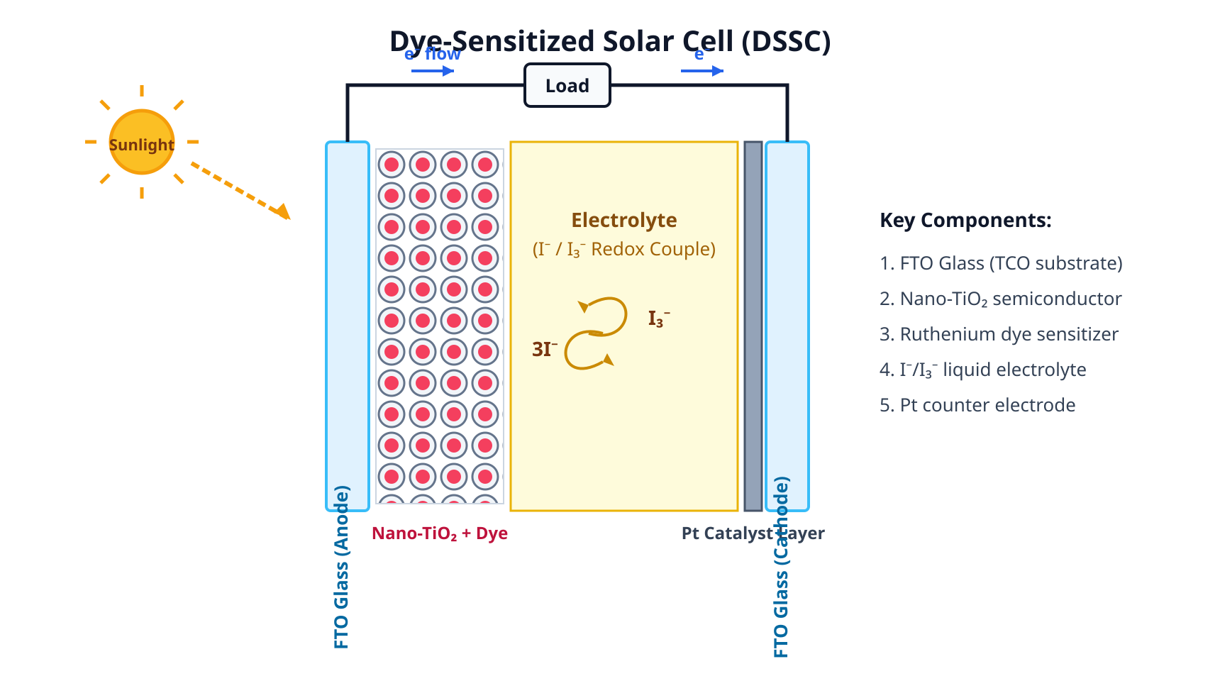
Figure: Cross-sectional schematic of a dye-sensitized solar cell showing the photoanode, dye-coated nanoporous semiconductor, redox electrolyte, and catalytic counter electrode.
Photoanode
The photoanode acts as the negative terminal during illumination and is formed by the transparent substrate, TCO collector, nanoporous film, and adsorbed dye monolayer.
Watch out. Do not confuse the chemical composition of transparent conductive oxides or the optical role of . FTO is fluorine-doped tin oxide (), not fluorine-doped indium tin oxide. Furthermore, has a wide band gap (, absorbing only ultraviolet light); it does not harvest visible sunlight on its own. Visible light is absorbed by the sensitizer dye, while nanoporous acts as a high-surface-area scaffold and electron transport medium. Also avoid listing as an electron-transport semiconductor: because its conduction band edge lies too high for electron injection from standard dyes, wide-band-gap may serve as an insulating reference, scaffold in a different architecture or a thin barrier, rather than an interchangeable TiO2 electron-transport layer.
Photoelectrochemical charge cycle
Because a DSSC operates as a galvanic cell under illumination, oxidation occurs at the photoanode and reduction occurs at the counter electrode (cathode). Electrical neutrality is maintained through a continuous four-step cycle:
- Photoexcitation of the dye: Incident photons pass through the transparent substrate and TCO layer and are absorbed by ground-state dye molecules () anchored to the surface. This promotes an electron from the highest occupied molecular orbital (HOMO) to the lowest unoccupied molecular orbital (LUMO), generating an excited state ():
- Electron injection and transport: Because the LUMO of the excited dye lies slightly higher in energy than the conduction band edge of , the excited electron is rapidly injected into the conduction band, leaving behind an oxidized dye cation ():
The injected electrons diffuse through the interconnected nanoparticle network to the TCO collector, flow through the external circuit to perform electrical work, and arrive at the counter electrode.
- Dye regeneration by the redox mediator: Before the injected electron can recombine with , iodide ions () in the electrolyte donate electrons to reduce back to its neutral ground state (), while iodide is oxidized to triiodide ():
Rapid regeneration prevents positive charge accumulation on the surface and resets the dye for repeated photon absorption.
- Electrolyte reduction at the counter electrode: Triiodide ions () diffuse across the electrolyte to the catalytic platinum or carbon counter electrode, where they pick up electrons returning from the external circuit to reform iodide ions:
where , , and denote the neutral ground-state, photoexcited, and oxidized sensitizer dye molecule, respectively, and represents an incident photon.
Watch out. The external wire carries electronic current. In the usual liquid electrolyte, charge transport involves mobile ions and redox-mediator transport and reactions, rather than a metallic stream of free electrons through the separator. Cell efficiency is governed by kinetic competition: electron injection and dye regeneration must occur much faster than parasitic recombination (where conduction-band electrons in fall back into or react directly with in the electrolyte).
Example 1: Tracing electron and ion stoichiometry in the iodide/triiodide cycle
Problem: During steady-state operation of a DSSC, two photons are absorbed by two adjacent sensitizer molecules on a nanoparticle. Write the balanced half-reactions and net chemical change to show how many electrons pass through the external load and how the electrolyte closes the circuit without net chemical consumption.
Solution:
-
Photoexcitation and injection (idealized two-photon cycle): Assume both absorbed photons produce successful excitation and electron injection, with no recombination losses:
Thus, enter the TCO photoanode and travel through the external load to the counter electrode.
-
Regeneration at the dye–electrolyte interface: Three iodide ions reduce the two oxidized dye cations back to neutral ground-state molecules:
-
Reduction at the counter electrode: The single ion diffuses to the Pt cathode and accepts the arriving from the external circuit:
-
Net cycle: Summing all steps cancels , , and on both sides. Two electrons are driven from the photoanode through the external load to the cathode per two absorbed photons, while both the dye and electrolyte are completely regenerated.
Advantages, limitations, and applications
Advantages
- Diffuse and low-light operation: Selected DSSCs perform well under diffuse or indoor light when the dye and cell design suit the source spectrum; comparison with silicon depends on the test conditions.
- Low-energy fabrication and architectural versatility: Roll-to-roll printing on polymer substrates enables lightweight, mechanically flexible cells, while glass-based cells can be made semi-transparent in varied colours.
Limitations and trade-offs
- Electrolyte sealing and thermal stability: Liquid organic electrolytes can volatilize at elevated outdoor temperatures or leak if perimeter seals degrade, motivating research into solid-state hole conductors and polymer gels.
- Dye cost, toxicity, and photostability: High-efficiency ruthenium complexes are expensive and rely on a scarce heavy metal, whereas natural plant pigments—whose toxicity, cost and stability depend on composition—suffer from rapid photodegradation and lower conversion efficiencies.
Applications
- Building-integrated photovoltaics (BIPV), such as semi-transparent power-generating windows, skylights, and architectural facades.
- Portable solar chargers integrated into outdoor fabrics, backpacks, and low-power indoor electronic sensors or illuminated signage.
Self-check questions
-
Why must the semiconductor oxide layer in a DSSC be nanoporous rather than a flat, dense film? Answer: Only dye molecules in direct contact with the surface can inject electrons into its conduction band, and a single flat monolayer absorbs very little incident sunlight. A mesoporous nanoparticle network can greatly increase the internal surface area, allowing enough dye to be anchored as a monolayer to harvest most incoming visible light.
-
What happens to cell output if the iodide/triiodide electrolyte dries out or freezes? Answer: Sustained photocurrent can fall sharply or cease when mediator transport is blocked. Without mobile ions to reduce , oxidized dye molecules cannot be regenerated and injected electrons rapidly recombine with instead of sustaining a continuous current through the external circuit.
Supercapacitors: interfaces, construction and energy storage
Supercapacitor
A supercapacitor (or ultracapacitor) is an electrochemical energy storage device that bridges the gap between conventional electrostatic capacitors and rechargeable batteries. It provides much higher capacitance than solid-state dielectric capacitors while charging and discharging far faster than batteries.
Supercapacitor serves as an umbrella term covering three primary device families:
- Electrical double-layer capacitors (EDLCs): Store charge electrostatically at the interface between a porous carbon electrode and an electrolyte without the charge-storage Faradaic reactions characteristic of pseudocapacitance.
- Pseudocapacitors: Store charge through fast, reversible Faradaic (redox) reactions at the surface of materials such as transition-metal oxides or conducting polymers.
- Hybrid supercapacitors: Combine an electrostatic EDLC electrode with a Faradaic or battery-type electrode.
Double-layer interfaces and charge storage
In an EDLC, energy is stored by separating charge across two solid–liquid interfaces. When a voltage is applied:
- The external circuit drives electrons from the positive electrode to the negative electrode.
- At the positive electrode, the excess positive electronic charge attracts solvated anions from the electrolyte.
- At the negative electrode, the excess negative electronic charge attracts solvated cations from the electrolyte.
- At each porous carbon surface, electronic charge in the solid faces an equal and opposite ionic counter-charge in the liquid, forming an electrical double layer only nanometres thick.
Because purely electrostatic EDLC storage requires no bulk phase change or electron transfer across the electrode–electrolyte interface, charging and discharging are rapid and highly reversible over hundreds of thousands of cycles.
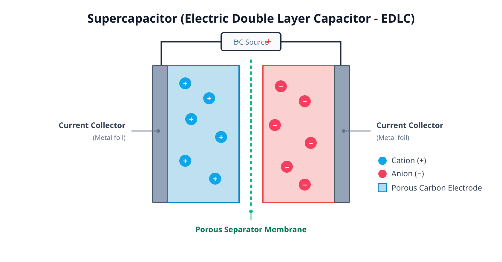
Figure 12.1: Structure of an electrical double-layer capacitor (EDLC) showing ion migration toward oppositely charged porous electrodes across an ion-permeable separator.
Device construction and materials
A practical supercapacitor cell consists of two porous electrodes, an electrolyte, a porous separator, current collectors, and polymer binders.
Electrodes
High-surface-area carbon nanomaterials—such as activated carbon, carbon nanotubes (CNTs), and graphene—form the backbone of EDLC electrodes, while metal-oxide nanoparticles or nanowires are added for pseudocapacitance. However, total geometric surface area alone does not determine capacitance: only ion-accessible pores that are properly wetted by the electrolyte and able to accommodate the electrolyte ions, sometimes with partial desolvation in narrow pores contribute to charge storage.
Electrolyte
The electrolyte supplies the mobile ions and sets the maximum operating voltage of the cell. Key electrolyte properties are high ionic conductivity, a wide electrochemical voltage window, and good pore wetting.
- Aqueous electrolytes (e.g., or solutions) offer high ionic conductivity and low cost, but water electrolysis limits their operating voltage to about .
- Organic liquid electrolytes—typically conductive salts such as tetraalkylammonium or lithium salts dissolved in organic solvents like acetonitrile or propylene carbonate—allow higher cell voltages ().
- Gel polymer electrolytes immobilize a liquid electrolyte in a polymer network. Solid electrolytes conduct ions through a solid phase; some are solvent-free polymer–salt systems. These formulations differ in conductivity and leakage behaviour.
Watch out. Do not confuse a salt dissolved in an organic solvent with a "solid electrolyte." A solvent mixed with tetraalkylammonium or lithium salts is a liquid organic electrolyte; true solid or gel electrolytes require a solid ceramic or polymer matrix. Furthermore, supercapacitor capacitance is governed primarily by accessible electrode surface area, ion size, and double-layer thickness—not simply the bulk dielectric constant of the electrolyte.
Separator
The separator (often a porous polymer or paper/cellulose membrane) sits between the two electrodes. It must be electrically insulating to prevent internal short circuits while remaining ion-permeable so cations and anions can migrate freely during charge and discharge. No electrons travel through the separator.
Current collectors and binders
Metallic foils or grids (such as , , , or carbon fibre) collect electrons from the electrodes and connect to the external terminals. Collector choice must match the electrolyte to avoid corrosion (for instance, aluminium is stable in organic electrolytes, whereas acidic aqueous solutions require corrosion-resistant carbon or noble metals). Polymer binders such as polyvinylidene fluoride (PVDF) or polyacrylonitrile (PAN) act as adhesives holding the active electrode particles together and onto the collector.
Capacitance, energy and power equations
The capacitance (in farads, ) relates stored charge (in coulombs, ) to the cell voltage (in volts, ):
Because a cell contains two electrode–electrolyte interfaces connected in series through the electrolyte, the total cell capacitance is related to the individual electrode capacitances and by:
For a symmetric cell where , the cell capacitance is half that of a single electrode (). Assuming constant capacitance, the total energy (in joules, ) stored at maximum voltage is:
Unlike a battery, which maintains a nearly flat voltage plateau during discharge, a supercapacitor's voltage drops linearly as charge is removed. The load and converter determine the minimum usable voltage , so the usable energy between and is:
Internal resistance—called equivalent series resistance (ESR)—arises from contact resistance, electrode resistance, and ion transport through pores. High ESR dissipates stored energy as heat () and limits peak power output.
| Feature | Supercapacitor (EDLC) | Rechargeable Battery |
|---|---|---|
| Charge storage mechanism | Electrostatic double layer (the EDLC case) | Bulk Faradaic (chemical redox) reactions |
| Specific power & charge rate | Very high (seconds) | Moderate to low (minutes to hours) |
| Specific energy | Lower | Higher |
| Cycle life | Very long ( cycles) | Limited by phase/volume changes |
| Discharge voltage profile | Sloping linearly with state of charge | Relatively flat voltage plateau |
| Self-discharge rate | Higher | Lower |
Example 1: Stored and usable energy in an organic-electrolyte cell
Additional illustrative example (not in source notes). Assume an ideal symmetric supercapacitor cell has a constant cell capacitance and a rated maximum voltage . Calculate (a) the total stored energy in joules and watt-hours, and (b) the usable energy and percentage of total energy recovered if the cell is discharged to .
-
Total stored energy at :
Convert joules to watt-hours ():
-
Usable energy down to :
-
Percentage of total energy delivered:
Because energy scales with , discharging to half the maximum voltage leaves of the initial energy remaining below the chosen operating cutoff.
Self-check questions
-
Question: Why does a symmetric supercapacitor whose single electrodes each have a capacitance of exhibit an overall cell capacitance of only ? Answer: The two electrode–electrolyte double layers are connected in series through the electrolyte, so , giving .
-
Question: What two electrical/transport properties must a supercapacitor separator simultaneously possess? Answer: It must be an electronic insulator (to prevent a short circuit between electrodes) and an ionic conductor/permeable membrane (to allow electrolyte ions to pass through).
Materials for quantum computing
Classical bits versus qubits
Classical bits
Classical digital processors store and manipulate information as binary bits, where each transistor switch occupies a definite voltage state corresponding to either or .
Qubits
Quantum computing encodes information in two-level quantum systems called quantum bits, or qubits. While a classical bit is strictly in state or at any instant, a single pure qubit can exist in a coherent linear superposition of two orthogonal computational basis states, written in Dirac notation as and :
Here, and are complex probability amplitudes (dimensionless) that carry both magnitude and phase. Physical measurement forces the qubit to project onto a single basis state: it yields outcome with probability and outcome with probability , subject to the normalization condition:
A register of qubits spans a composite state space (Hilbert space) described by complex probability amplitudes simultaneously.
Watch out. Superposition does not mean that a single qubit holds all numbers from to , nor does it allow a quantum computer to read out all possible answers at once. Representing basis states requires an -qubit register (), and a single measurement of that register collapses the state to yield only one -bit binary string. Quantum computers are not universally faster for every task; useful speedups depend on specialized algorithms that manipulate amplitudes before measurement.
Core quantum phenomena in computation
Quantum algorithms process information by combining three fundamental physical properties:
- Superposition: A quantum system evolves as a coherent linear combination of basis states with well-defined relative phases; measurement produces an outcome, while coupling to the environment can destroy observable coherence.
- Entanglement: Two or more qubits can enter a non-separable joint quantum state whose total state vector cannot be factored into individual single-qubit states. Measuring one entangled qubit establishes strong non-classical correlations with the measurement outcomes of its partner qubits, though it cannot transmit information faster than light.
- Quantum interference: Because and are complex numbers with relative phases, quantum logic gates can steer probability amplitudes so that paths leading to wrong answers interfere destructively (cancel out) while paths leading to target answers interfere constructively (reinforce the measurement probability).
To execute these operations reliably, qubits must maintain phase relationships over a characteristic coherence time. Unwanted thermal, electromagnetic, or spin interactions with the surrounding lattice cause decoherence, which destroys superposition and introduces computational errors that require quantum error correction.
Example 1: State space and measurement of an 8-qubit register (illustrative conceptual example)
Problem: An engineering student reads that a quantum processor with qubits can evaluate numbers in parallel. Assuming an ideal -qubit register prepared in an equal superposition of all computational basis states, determine (a) how many basis states span the register, (b) the probability of obtaining any specific -bit outcome in a single measurement, and (c) how the full probability distribution is obtained experimentally.
Solution:
- Basis states: For qubits, the dimension of the state space is: These correspond to binary strings from (decimal ) to (decimal ).
- Single-measurement outcome: In an equal superposition, every basis state has magnitude . A single measurement collapses the register to just one -bit string with probability:
- Experimental readout: Because one measurement returns only one binary number, the circuit must be re-initialized, run, and measured repeatedly over many shots to build a statistical histogram of output probabilities.
Physical platforms and material requirements
Qubits are not limited to electron spins; different hardware architectures encode and in superconducting circuits, semiconductor spins, crystal defects, or photons. In every platform, materials chemistry governs coherence because interface oxides, lattice vacancies, and nuclear-spin impurities create charge and magnetic noise that dephase the qubit.
| Qubit platform | Representative materials | Physical role and material engineering requirements |
|---|---|---|
| Superconducting circuits | Aluminium (), niobium (), titanium nitride () on high-resistivity silicon or sapphire | Form zero-resistance microwave resonators and Josephson junctions () operating at millikelvin temperatures; clean metal–substrate interfaces minimize dielectric two-level-system losses. |
| Semiconductor spin qubits | Isotopically purified silicon (), , germanium (), or heterostructures | Confine single electron, hole, or nuclear spins in gate-defined quantum dots; isotopic enrichment of removes nuclear spins that otherwise cause magnetic decoherence. |
| Solid-state colour centres | Diamond (nitrogen-vacancy, centres) and silicon carbide () | Point defects trap localized electronic spins that can be initialized and read out optically at or near room temperature. |
| Photonic quantum systems | quantum dots; silicon nitride () and lithium niobate () waveguides | Self-assembled dots act as on-demand single-photon emitters, while ultra-low-loss dielectric waveguides route photons for quantum communication and linear optical computing. |
Self-check questions
- Question: A qubit is prepared in the state . Verify whether the state is normalized and find the probability of measuring . Answer: The probabilities are and . Since , the state is normalized, and the probability of measuring is ().
- Question: Why is isotopically enriched preferred over natural silicon for semiconductor spin qubits? Answer: Natural silicon contains isotopes with non-zero nuclear spin, creating fluctuating local magnetic fields that rapidly decohere the electron spin qubit; has zero nuclear spin, providing a magnetically quiet lattice.
Spintronics and magnetoresistive devices
Principles of spintronics
Conventional electronics relies exclusively on the electrical charge of electrons to process and store data.
Spintronics
Spintronics (spin-based electronics) exploits both the charge of an electron and its intrinsic spin—a quantum mechanical angular momentum that gives each electron a tiny magnetic moment. Spin is an intrinsic quantum property rather than a literal physical rotation of a sphere.
In an external magnetic field or inside a ferromagnetic material, electron spins align predominantly in one of two states, referred to as "spin-up" and "spin-down". When an unequal number of spin-up and spin-down electrons carry current, the current is spin-polarized. Controlling spin polarization allows solid-state devices to store data in magnetic orientations. Because ferromagnetic magnetization remains stable without continuous electrical power, magnetic spin states enable non-volatile data storage. While an individual electron's spin polarization in a conduction channel relaxes quickly, collective magnetization in a ferromagnet can retain data without continuous power, subject to thermal stability, retention time, and device design.
Magnetoresistive phenomena
Spintronic sensors and memories read magnetic states by converting relative magnetization alignments into electrical resistance changes.
Giant magnetoresistance (GMR)
Giant magnetoresistance (GMR) occurs in thin-film heterostructures composed of alternating ferromagnetic conducting layers separated by a nanometer-thin non-magnetic metallic spacer (such as Cu). Resistance changes because of spin-dependent scattering at the interfaces and within the layers:
- Parallel alignment (): When the magnetizations of both ferromagnetic layers are parallel, electrons with spin aligned to the magnetization pass through both layers with minimal scattering, resulting in low electrical resistance.
- Antiparallel alignment (): When the magnetizations are antiparallel, both spin-up and spin-down electrons undergo strong scattering in at least one of the ferromagnetic layers, resulting in high electrical resistance.
Practical devices use a spin valve architecture: one ferromagnetic layer has its magnetization fixed (pinned layer) by an adjacent antiferromagnetic layer, while the other ferromagnetic layer (free layer) rotates freely in response to a small external magnetic field.
Tunnel magnetoresistance (TMR)
Tunnel magnetoresistance (TMR) occurs in a magnetic tunnel junction (MTJ), where two ferromagnetic electrodes are separated by an ultrathin insulating tunnel barrier (typically or , only thick) rather than a conductive metal. Electrons cross the barrier by quantum mechanical tunneling. Because tunneling probability depends strongly on the matching of spin-polarized density of states between the two electrodes, well-designed MTJs can provide large resistance changes, with the result depending on the materials and operating conditions.
| Feature | Giant Magnetoresistance (GMR) | Tunnel Magnetoresistance (TMR) |
|---|---|---|
| Device structure | Ferromagnet / non-magnetic metal / ferromagnet | Ferromagnet / thin insulator / ferromagnet (MTJ) |
| Typical spacer / barrier | Conductive metal (, ) | Insulating oxide (, ) |
| Conduction mechanism | Ohmic transport with spin-dependent scattering | Spin-polarized quantum tunneling |
| Typical applications | Early high-density HDD read heads, magnetic field sensors | Modern HDD read heads, MRAM cells |
Watch out. Do not classify and as metallic spintronic materials, and do not group metallic alloys as semiconductors. and are electrical insulators used as tunnel barriers in MTJs, whereas , , and are metallic ferromagnets.
Example 1: Illustrative calculation of magnetoresistance ratio
Additional illustrative example. Suppose a spin-valve sensor has a resistance of when its ferromagnetic layers are aligned parallel, and when they are aligned antiparallel. Calculate the magnetoresistance (MR) ratio using the standard optimistic convention.
Solution: Using the parallel resistance as the reference denominator:
Substitute and :
The resistance increases by when switching from the parallel to the antiparallel state.
Material classes in spintronics
- Metallic ferromagnets and insulators (metal/insulator stacks): Ferromagnetic transition metals and alloys such as , , , and amorphous provide high spin polarization at room temperature. They are paired with non-magnetic metals () in GMR devices or crystalline oxide insulators (, ) in TMR devices.
- Semiconductor-based materials: Conventional semiconductors (, , ) allow spin transport and manipulation via electric fields. Diluted magnetic semiconductors (DMS), such as or doped with manganese (, ), combine semiconducting tunability with ferromagnetism, though most DMS materials only exhibit ferromagnetism well below room temperature.
- Graphene-based materials: Graphene serves as an exceptional non-magnetic spin-transport channel in part because carbon has low atomic number and intrinsic spin–orbit coupling is weak. This allows spin-polarized currents to travel micrometre-scale distances with minimal spin scattering.
Applications
- Hard disk drive (HDD) read heads: GMR spin-valve sensors revolutionized magnetic recording in the late 1990s by detecting tiny magnetic bits on spinning platters; modern high-density HDDs use higher-sensitivity TMR read heads.
- Magnetoresistive random-access memory (MRAM): Stores binary bits ( and ) as parallel or antiparallel magnetization states in arrays of MTJs (using TMR). MRAM is non-volatile, fast, and can reduce the energy required to retain the stored bits; peripheral circuitry still consumes power.
- Magnetic field sensors: Used in automotive anti-lock braking rotors, industrial position encoders, and biosensors.
Self-check questions
- Why does an antiparallel alignment of ferromagnetic layers in a GMR spin valve produce higher resistance than a parallel alignment? Answer: In the parallel state, one spin channel matches the magnetization of both layers and passes through with weak scattering (forming a low-resistance path). In the antiparallel state, both spin-up and spin-down electrons encounter an oppositely magnetized layer and experience strong scattering.
- What is the structural difference between a GMR stack and a TMR magnetic tunnel junction? Answer: A GMR stack separates its two ferromagnetic layers with a thin conductive non-magnetic metal (like ), whereas a TMR junction separates them with an ultrathin insulating barrier (like or ) through which electrons must tunnel.
Revision sheet and practice problems
Core definitions and relationships
| Concept | Definition / Key Relationship | Governing Equation / Metric |
|---|---|---|
| Nanomaterial classification | Materials with nanoscale external dimensions or internal features, typically around . | 0D: all 3 dims (fullerenes, CQDs); 1D: 2 dims (CNTs, nanowires); 2D: 1 dim (graphene, nanofilms); 3D: 0 external dims , nano-structured bulk |
| Surface-to-volume ratio | Ratio of surface area () to volume () for a sphere of diameter ; drives high surface reactivity as decreases. | |
| Euler's polyhedron formula | Relates vertices (), edges (), and faces () in closed convex cage molecules such as fullerenes. | |
| OLED photon emission | Energy of light emitted when an electron drops from the LUMO to a hole in the HOMO. | ; (: Planck's constant, : speed of light, : wavelength) |
| Supercapacitor energy | Electrostatic energy () stored in a cell of capacitance at voltage ; converted from joules to watt-hours. | ; |
| Qubit state space | An -qubit register exists in a linear superposition of computational basis states prior to measurement. | Basis states ; Each single measurement collapses the state to 1 classical bit-string outcome. |
| Magnetoresistance (MR) | Relative electrical resistance change between antiparallel () and parallel () ferromagnetic alignments. |
Watch out. Do not confuse excitation with emission in organic electronics, or superposition with classical parallel output. In an OLED, radiative recombination is a LUMO HOMO decay (not HOMO LUMO). In quantum computing, an -qubit superposition holds amplitudes simultaneously, but measuring the register yields only one bit-string per run.
Rapid-fire retrieval Q&A
-
Is molecular fullerene () harder than diamond?
No. Individual cages have strong covalent bonds, but solid fullerite crystals are held together by weak van der Waals forces, making ordinary bulk a comparatively soft molecular solid. -
What is the exact geometry of ?
It is a truncated icosahedron ( faces: isolated pentagons and hexagons, with -hybridized carbon vertices and two distinct C–C bond lengths), not a regular -faced icosahedron. -
Are all carbon nanotubes metallic conductors?
No. Electronic behavior depends on the chiral vector : armchair CNTs () are metallic, whereas zigzag () and chiral () CNTs are nominally metallic in the zone-folding model if is a multiple of , and semiconducting otherwise. Curvature can open a small gap in non-armchair tubes. -
How does doping polyaniline (PANI) differ from doping polyacetylene?
Polyacetylene is doped via redox reactions ( oxidation or sodium naphthalide reduction), whereas emeraldine base PANI is converted to the conducting emeraldine salt via acid protonation () without changing the average oxidation state of the backbone. -
Do flame-retardant polymers make materials completely fireproof?
No. They are flame-retardant, meaning they slow ignition, reduce heat release, and quench gas-phase free radicals (, ) or form protective char to provide escape time, but they can still degrade under sustained heat. -
Which orbital transition produces light in an OLED?
Electroluminescence occurs via radiative LUMO HOMO relaxation (exciton recombination) in the emissive layer after electrons are injected from the cathode and holes from the anode. -
In a DSSC, which component absorbs sunlight and which transports electrons?
The photosensitizer dye absorbs visible light and injects photoexcited electrons into the conduction band of the wide-band-gap semiconductor, while the counter electrode (Pt/graphite) reduces back to in the electrolyte. -
What is the role of the separator in an electrical double-layer capacitor (EDLC)?
It physically prevents electrical contact and electron flow between the electrodes while remaining porous to allow electrolyte ions to migrate freely during charging and discharging. -
Does an -qubit quantum register output numbers at once when read?
No. An -qubit system spans basis states in superposition, interference changes their probabilities during gate operations, but a single readout collapses the register to one -bit value. -
How do GMR and TMR spin valves differ in construction?
Giant Magnetoresistance (GMR) uses a thin non-magnetic metal spacer (such as ) between ferromagnetic layers, whereas Tunnel Magnetoresistance (TMR) uses an ultrathin insulating oxide barrier (such as or ) through which spin-polarized electrons quantum-mechanically tunnel.
Numerical practice problems
-
(Additional illustrative example) Assume a bulk sample of spherical nanoparticles of diameter is dispersed into smaller spherical nanoparticles of diameter while conserving total material volume. Calculate the factor by which (a) the surface-to-volume ratio increases and (b) the total number of particles increases.
Solution: For a sphere of diameter , the surface-to-volume ratio is .
Since total volume is constant, the particle count scales inversely with :
The surface-to-volume ratio increases by a factor of , and the particle count increases by a factor of .
-
(Additional illustrative example) A fullerene cage has carbon vertices, each forming covalent bonds along the polyhedral edges. Calculate the total number of edges and use Euler's polyhedron formula to find the total number of ring faces .
Solution: Each edge connects vertices, so bonds per vertex yields:
Applying Euler's formula ():
The cage has edges and faces ( pentagons and hexagons).
-
(Additional illustrative example) An electrical double-layer supercapacitor cell has a capacitance of and is charged to a cell voltage of . Calculate the stored energy in joules () and in watt-hours ().
Solution: Using the electrostatic energy equation:
Converting joules to watt-hours ():
The supercapacitor stores (or ).
-
(Additional illustrative example) A quantum processor register contains entangled qubits. Determine the number of computational basis states in its superposition space and state how many classical bit strings are obtained from a single projective measurement.
Solution: The dimension of the basis state space for qubits is :
Upon measurement, wavefunction collapse projects the superposition onto a single eigenstate. Thus, basis states can be represented in superposition, and one -bit classical string is returned per measurement.
-
(Additional illustrative example) A spintronic read-head sensor exhibits a resistance of when its ferromagnetic layers are aligned parallel and when aligned antiparallel. Calculate the magnetoresistance ratio () as a percentage.
Solution: Using the optimistic magnetoresistance definition:
The magnetoresistance of the sensor is .
Long-answer review prompts
Use these structured prompts to verify mastery across all Module 2 topics:
- Nanomaterials and Synthesis: Classify nanomaterials by dimension () and composition (carbon, metal/oxide, nanocomposites, dendrimers, biological), and write balanced chemical equations for preparing nano- via alkoxide sol–gel hydrolysis/polycondensation and metallic nanoparticles via chemical reduction, distinguishing a reduction half-reaction from a complete synthesis equation.
- Graphene and Carbon Quantum Dots (CQDs): Explain how hybridization and delocalized () orbitals govern the electrical, thermal, and mechanical properties of graphene; compare top-down and bottom-up routes for synthesizing graphene and fluorescent CQDs ().
- Fullerenes and Carbon Nanotubes (CNTs): Compare the cage structure of with single-walled (armchair, zigzag, chiral) and multi-walled (Russian doll, parchment) CNTs, relating their synthesis (arc discharge, laser ablation, CVD) and geometry to electronic and energy-storage applications.
- Polymer Classification and Flame Retardancy: Distinguish addition vs. condensation polymers and homopolymers vs. copolymers; explain how halogenated polymers (PVC, polybromostyrene) quench gas-phase combustion radicals () and how non-halogenated char-forming polymers (novolac, bakelite, polyimide, polybenzoxazole) slow flame spread.
- Conducting Polymers, PANI, and PPy: Contrast intrinsically conducting polymers (conjugated -backbones, -doping with , -doping with sodium naphthalide) with extrinsically conducting polymers (filled and blended); outline the chemical and electrochemical oxidative polymerization of polyaniline (PANI) and polypyrrole (PPy) and identify emeraldine salt as the conducting form of PANI.
- Organic Light-Emitting Diodes (OLEDs): Sketch the multilayer OLED architecture (substrate, ITO anode, a suitable hole-injection/transport layer, polyfluorene/PPV emissive layer, metallic cathode) and explain charge injection, hole/electron migration, and radiative exciton recombination.
- Dye-Sensitized Solar Cells (DSSCs): Diagram a DSSC and trace the complete closed-loop charge cycle: dye photoexcitation, electron injection into mesoporous nano-, external circuit work, dye regeneration by , and reduction at the counter electrode.
- Supercapacitors, Quantum Computing, and Spintronics: Compare electrostatic double-layer charge storage in porous carbon supercapacitors with battery storage; summarize how superposition, entanglement, and interference operate in superconducting (Al, Nb, TiN), spin (Si), and photonic (InAs, GaAs) qubits; and explain how spin polarization and magnetoresistance (GMR/TMR) enable non-volatile magnetic memory and sensors.
Learning checklist
- Explain a material’s structure before listing its properties and applications.
- Distinguish ideal models from real samples, formulations and devices.
- Trace electrons, holes and ions separately in each device.
- State units, assumptions and the reference denominator in every calculation.